
Back to blog
DFM Checks Enhance PCB Design and Reduce Production Errors

DFM Checks
Avoiding a premium for custom PCBs is a primary concern, and understandably so. The overall manufacturing cost of PCBs encompasses various factors. Apart from fixed expenses like logistics, labor, and equipment, fluctuations are primarily driven by factors such as board dimensions, material selection, and process technology. These variables hinge upon the decisions made by engineers during the design phase.
To ensure seamless manufacturability of the circuit board design, minimize production expenses, enhance manufacturing efficiency, and uphold the ultimate product quality, the concept of Design for Manufacturability (DFM) emerged as a pivotal force in the PCB domain. In this comprehensive guide, we’ll delve deeply into this subject, equipping you to augment project profitability. Let’s get started.
Integrating DFM checks into the PCB manufacturing process flow is crucial for ensuring that each stage—aligns perfectly with manufacturing capabilities and product requirements. By viewing a detailed video on the PCB Manufacturing Process Flow, engineers and designers can visualize exactly where DFM checks can be most effectively implemented. This helps in identifying potential issues early on.
What is Design for Manufacturing (DFM)?
Design for Manufacturing (DFM) is all about making sure that the manufacturing process of your PCBs is as smooth and cost-effective as possible. The main goal here is to optimize dimensions, materials, tolerances, and functionality by using the most efficient manufacturing methods available. This process should start early, even before sketching begins. Aligning PCB design for manufacturing with the initial concept of the device is crucial, with a primary focus on understanding how the customer will use it. Investing significant time and effort into developing a solid DFM process will yield substantial benefits later in the design phase.
Optimizing Component Costs
Component costs are a big deal in any circuit board project. Partnering with a PCBA company like Highleap Electronic, which has an in-house engineering team, allows for leveraging DMFA (Design for Manufacturing and Assembly) techniques. This helps identify the best component alternatives, simplifies design and manufacturing, and keeps component procurement expenses in check.
Design Upgrade
Connecting with manufacturers, including printed circuit board manufacturers and casing suppliers, or seeking advice from industrial designers can be incredibly helpful. Continuously asking questions like “Can this be improved?” and discussing how your electronic or PCB designers have tackled similar issues in the past can offer valuable insights. When kicking off the DFM process, try to anticipate potential challenges, set up a design sequence, outline potential obstacles at each step, and then look at similar products. Analyze how similar issues were resolved and strive to implement those solutions.
Fostering Collaboration
DFM is not just about the design; it’s about fostering collaboration between manufacturers and customers. This means defining responsibilities for both sides to address and resolve design-related issues, preventing flawed board production and reducing conflicts. Engaging all stakeholders—electronic engineers, PCB designers, industrial designers, PCBA manufacturers, mold makers, and material suppliers—in the DFM process is crucial. This cross-functional approach ensures that the design is created without incurring unnecessary costs. Collaborating across departments ensures timely identification and resolution of defects before they become major issues.
Cost-Efficiency
Implementing an early PCB DFM check significantly reduces expenses associated with design alterations later in the product development cycle. As the design evolves, making changes becomes progressively more expensive and challenging due to their increasing complexity. DFM helps engineers identify materials that strike a balance between optimal performance and cost-effectiveness, avoiding unnecessary costs. One of DFM’s key features is integrating designs that maximize the utilization of raw materials while enhancing the product’s aesthetic intricacies. Importantly, DFM contributes to optimizing the manufacturing process, allowing for the re-evaluation of previous projects and the elimination of unnecessary steps in the production pipeline.
Restoration Design
When developing a new product, involving stakeholders in the product development process from the beginning is simpler. However, even when creating a new version of an existing product, a comprehensive PCB design for manufacturing checklist remains indispensable. Design errors often recur when replicating a previous design, so scrutinize and question every facet of your design during the DFM process.
Check")
PCB DFM Checks
PCB Design For Manufacturing Checklist
Usage Cycle
Thoroughly analyzing how users will interact with the product is crucial. This involves meticulous planning of the PCB assembly process to ensure efficient assembly steps and optimal tool utilization. Deciding on the appropriate soldering method (such as surface mount technology or through-hole soldering), determining the optimal component placement orientation, refining routing, and ensuring both assembly speed and quality are all essential considerations. Incorporating automated equipment can enhance assembly speed, and strategic layout optimization can reduce assembly errors.
When building prototypes, there’s no need to use materials with aerospace-level requirements or opt for fabrication with high environmental certifications. Similarly, complex board shapes aren’t necessary if you’re producing small quantities. Unless the design explicitly demands it, as it involves creating tools and dies for manufacturing low-volume parts, which increases the cost of PCB prototyping.
It’s important to consider factors like the quantity of parts to be manufactured, the choice of materials, required finishes, tolerances, and the need for secondary processes.
Design
The design phase forms the backbone of the product ideation process, requiring consideration of all necessary conditions. This stage encompasses electronic circuit design, PCB layout, connector placement, and collaboration with industrial designers to strategically position indicators, control buttons, connectors, and cables associated with the printed circuit board. Components should not be oversized in either dimensions or electronic capability. Proper component selection should adhere to electronic design standards by choosing components capable of withstanding at least twice the capacity they will be used for.
Tracks should be appropriately sized to handle the expected current load. Signal tracks should be compact to avoid unnecessary space consumption. Precise dimensional tolerances should be defined.
For boards intended for automated assembly by pick-and-place machines, fiducials should be added to expedite the manufacturing process. Consult with your manufacturer to determine if tooling holes are necessary. It’s essential to collaborate with your contract manufacturer to ensure your design aligns with sound manufacturing principles for PCBA fabrication.
Materials
Selecting the right materials is paramount in PCB design for manufacturing. This includes considerations for heavier weight copper (commonly 1oz or 2oz), PCB substrate material thickness (e.g., aluminum or FR4 material), and overall board thickness, which varies from 0.4 mm to 2 mm depending on the application. For instance, RF designs might necessitate thinner PCBs. Highleap Electronic strongly recommends referring to resources like the PCB copper thickness guide and related documents during the developmental phase. The PCB DFM guidelines examine various material aspects:
- How strong should the material be?
- Should the solder mask have a specific color? The silkscreen generally needs to contrast with the mask.
- How heat-resistant does it need to be?
- Will the board carry significant current? Will there be high voltage? Track thickness should be considered for current calculations, and gap spacing for voltage calculations.
- How flame-resistant should the material be?
- What thickness is required? What substrate material is best? Is FR4 suitable, or is better heat dissipation needed, possibly using aluminum?
Once again, ensure you discuss the material with your PCB manufacturer, exploring their compatible inventory materials, which can help secure lower material costs.
Environment
Your product’s design must account for the environment it will be exposed to. Will the board be used in a harsh environment with vibrations, high temperatures, sun exposure, high humidity, or flammable atmospheres? This involves addressing potential issues like dust, humidity, and corrosion. Additionally, it’s crucial to assess whether the circuit requires features like high-frequency operation or miniaturization.
The manufacturer’s environmental certifications, including RoHS certification and electromagnetic interference resistance certification, should be thoroughly evaluated. Industries with specific attributes should also verify manufacturer qualifications, such as ISO13485 (medical) or IATF16949 (automotive) certifications.
Compliance/Testing and Calibration
Defining the battery of tests or analyses that the printed circuit board will undergo before assembly is crucial. This is especially important for larger boards with numerous components or high manufacturing costs, as these tests ensure that no electronic flaws are overlooked. These tests can align with laboratory PCB tests aimed at securing certifications like the ones mentioned earlier.
With the exception of some prototypes produced in low quantities, all products must meet safety and quality standards. These standards can be IPC PCB standards, regional standards, or internal standards specific to the company or to you as a customer.
Do you require any ISO certification? Who will provide UL testing, ETL, and others? Who will conduct and where will such testing take place?

CAM engineer inspects gerber files
Design Flaws for DFM Checks
Edge Gap
Proper allocation of edge clearance is essential to prevent coating removal issues during PCB cutting. Incorporating additional dimensions for protective coating ensures the integrity of the copper layer and minimizes the risk of corrosion.
Acid Trap
Sharp angles in trace corners can lead to acid trap formation during the etching process. Implementing chamfers or bevels and avoiding acute angles can mitigate acid trap issues and ensure smooth flow during immersion.
Absence of Solder Mask
The omission of a solder mask layer poses a significant risk of unintended contact between pads, resulting in circuit board short-circuit incidents. Integrating the protective layer into design protocols ensures optimal protection and reliability.
Optimizing Via Placement
Strategic placement of vias can help liberate valuable space on the PCB. However, excessive deployment of vias can compromise soldering efficacy. Careful consideration of via types and placement is essential to avoid detrimental effects on board performance.

PCB DFM Check
Factors Affecting Design for Manufacturing
In addition to the aforementioned considerations, several other factors can impact PCB design and assembly:
Reducing Parts
Using fewer materials reduces the need for engineer intervention, shortens production processes, lowers labor requirements, and potentially reduces shipping costs.
Standardizing Elements
Standardizing PCB board dimensions and shapes that can be used across different devices or designing boards that can serve multiple functions based on the installed components is a cost-effective approach.
Implementing Modular Assemblies
Building upon commercial modules and non-customized designs allows for smoother and more cost-effective product modifications.
Easy Connections
Minimize the need for numerous PCB connectors, which can increase costs. If required, opt for commercial connectors. Use standard connectors whenever possible, employ self-tapping screws for quicker placement, and avoid overly long or thick screws, split washers, threaded holes, special heads, and those needing specific tools.
Connector Alternatives
While the above points offer optimization solutions for connectors, it’s recommended to consider alternatives such as rigid-flex PCBs. Though more expensive in manufacturing, they provide improved features and reduce overall project costs.

CAM engineer DFM Checks
Why Choose Highleap Electronic for Your Next Electronic Project?
As an experienced engineer, I highly recommend selecting Highleap Electronic for your next electronic project. Firstly, Highleap Electronic boasts a highly skilled engineering team proficient in Design for Manufacturing (DFM) principles. By partnering with us, you can receive valuable advice during the design phase to optimize your circuit board design, reduce production costs, enhance manufacturing efficiency, and ensure the highest quality of the final product.
Secondly, Highleap Electronic has extensive experience in handling complex PCB and PCBA projects. Our team excels not only in designing and manufacturing high-density, multi-layer circuit boards but also in handling various materials and special processes. Whether your project involves high-frequency, high-current, or high-temperature environments, we have the solutions and certifications, such as ISO13485 (medical) and IATF16949 (automotive), to meet your specific industry requirements.
Conclusion
In conclusion, PCB design for manufacturing (DFM) is all about meticulous planning, strategic collaboration, and continuous optimization. By adhering to DFM principles, you can significantly enhance manufacturability, reduce costs, and improve the overall quality of your PCBs. Whether you’re new to PCB procurement or a seasoned professional, integrating DFM checks into your design process is crucial for achieving optimal results.
Unlock the potential of PCB design for manufacturing with Highleap Electronic – your trusted partner in premium PCB assembly services.
DFM Checks FAQ
1.How can I ensure my PCB design will not create acid traps during manufacturing?
To avoid acid traps, ensure that your trace angles are at least 90 degrees and avoid sharp corners. Consider using chamfers or beveled edges when connecting traces to ensure smooth flow during the etching process, reducing the risk of residual acid buildup.
2.What factors should I consider when selecting materials for my PCB?
When selecting PCB materials, consider factors such as strength, heat resistance, conductivity, and flame retardance. Depending on the specific application (e.g., high-frequency operations or harsh environments), choose suitable substrates like FR4 or aluminum. Discuss with your manufacturer to ensure the chosen materials optimize both cost and performance.
3.How can I ensure the edge clearance of my PCB design does not compromise the integrity of the protective coating?
In your design, allocate sufficient edge clearance. For the outer layers, an additional 0.010 inches of coating area is recommended, and for the inner layers, an additional 0.015 inches is advised. This ensures the protective coating remains intact during the PCB cutting process, preventing copper layer exposure and potential corrosion.
4.How can I optimize the placement of vias in my PCB design?
Consider space constraints and soldering effectiveness when placing vias. Avoid overusing vias to prevent solder wicking. Choose the appropriate via type (e.g., microvias, blind vias, buried vias) based on your design needs and ensure their placement does not interfere with other components’ installation and operation.
5.What should I consider in PCB design for harsh environmental conditions to ensure reliability?
If your PCB will be exposed to harsh conditions like high temperatures, humidity, or vibrations, select materials with excellent heat resistance and moisture protection. Add protective coatings or shielding to prevent dust, humidity, and corrosion. Ensure your design meets relevant environmental certifications such as ROHS and EMI resistance to enhance reliability.
By implementing these DFM checks, you can significantly improve the manufacturability of your PCB design, reduce production costs, and ensure the quality and reliability of the final product. Partnering with Highleap Electronic guarantees you top-notch technical support and manufacturing services, ensuring the success of your electronic project.

Related Articles
Future Prospects and Challenges in Local Oscillator Development
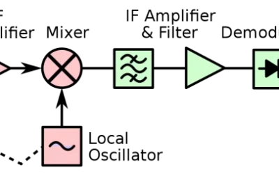
Developing multi-function chips that integrate local oscillators(LOs) with other RF components, such as mixers, amplifiers, and filters, is an emerging trend.

Understanding Silkscreen on PCB: A Comprehensive Guide for PCB Manufacturers
We will dive deep into the world of PCB silkscreen, exploring its significance, printing methods, design considerations, and much more.

What is the use of decoupling capacitors in PCB?
Decoupling capacitors, also known as bypass capacitors, are used to filter noise from power lines and stabilize voltage levels on ICs.
Take a Quick Quote