
Back to blog
Mastering PCB Cost Estimation: A Comprehensive Guide

In the evolving landscape of electronics manufacturing, understanding the intricacies of Printed Circuit Board (PCB) cost estimation stands as a cornerstone for success. This detailed guide provides an in-depth analysis of the factors influencing PCB costs, offering valuable insights for engineers, designers, and procurement specialists alike. By embracing a thorough approach to PCB cost estimation, organizations can navigate the complexities of manufacturing processes, material selection, and design considerations, ensuring both cost-efficiency and high-quality outcomes.
Key Factors Influencing PCB Cost
PCB Size and Complexity
Dimensional Parameters:
Larger PCBs require more materials and extended production time, influencing the overall cost.
Layer Count:
Increasing the number of layers in a PCB design adds to the complexity and the price, given the additional processing and materials needed.
Material Selection
Substrate Materials:
Choices range from standard FR-4 to high-performance materials like Rogers for specific applications, affecting both cost and performance.
Copper Thickness:
Thicker copper layers, necessary for high-power applications, can significantly impact the cost due to material usage and processing time.
Surface Finish Types
Options:
From HASL (Hot Air Solder Leveling) to ENIG (Electroless Nickel Immersion Gold), the choice of surface finish affects durability, conductivity, and price.
Considerations:
Selection depends on the required electrical performance, environmental resistance, and compatibility with subsequent assembly processes.
Manufacturing Volume
High-volume orders typically reduce the unit cost due to economies of scale, whereas low-volume runs incur higher per-unit costs because of setup and teardown expenses.
Design Complexity and Features
Intricacies:
Advanced features like blind and buried vias, tight tolerances, and unique shapes add to the production challenges, reflecting on the cost.
Design Optimization:
Efficient design practices can mitigate costs, emphasizing the importance of early cost estimation in the design phase.
For a more complete production review, use this article alongside circuit board cost review and immersion gold PCB when checking stackup, assembly, or test requirements.
PCB Cost Estimation Process
Accurate PCB cost estimation is a multifaceted process, involving detailed analysis of design specifications, material requirements, and manufacturing capabilities.
- Initial Design Review: Evaluating the PCB design for complexity, size, and layer count.
- Material Selection: Choosing appropriate substrates and copper thickness based on performance requirements.
- Surface Finish Determination: Selecting a surface finish that balances cost with functional needs.
- Volume Assessment: Estimating the production volume to leverage scale effects.
- Manufacturing Capability Analysis: Ensuring the selected manufacturer can meet the design specifications and quality requirements.
- Leveraging Technology for Enhanced Accuracy
- Advanced software tools and PCB cost estimation calculators play a pivotal role in streamlining the estimation process, offering real-time insights and adjustments based on varying parameters.
Strategic Approaches to Cost Optimization
Beyond mere estimation, strategic planning and optimization are vital for minimizing PCB manufacturing costs without compromising quality.
- Early Cost Estimation: Integrating cost considerations in the early stages of design to guide material and process decisions.
- Design Simplification: Reducing complexity where possible to lower production challenges and costs.
- Material Rationalization: Selecting cost-effective materials that meet the required specifications.
- Volume Planning: Balancing order volumes to achieve optimal pricing through scale advantages.

Related Articles
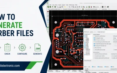
How to Generate Gerber Files for PCB Manufacturing
Learn how to generate Gerber files in Altium, KiCad, and EAGLE, which outputs belong in the package, and how to avoid fab delays.
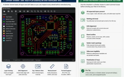
Gerber File Review Checklist: How to Check PCB Files Before You Order
Check Gerber files before PCB ordering: copper layers, drills, outlines, solder mask, silkscreen, panel data, and common file errors.
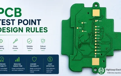
PCB Test Point Design Rules for Debug and ICT
Learn how to place PCB test points for debug, flying probe, and ICT access without sacrificing routing density or assembly reliability.