
Back to blog
Solder Mask Mastery: Boosting PCB Durability & Function

Solder Mask PCB in different colors
In the realm of printed circuit board (PCB) manufacturing, the solder mask is a pivotal element, ensuring not only the aesthetic appeal of the board but also its functionality and longevity. This comprehensive guide delves into the intricacies of solder masks, offering insights into their importance, types, application processes, and the key role they play in PCB design and performance.
Understanding Solder Masks
A solder mask, often referred to as solder resist, is a protective coating applied to the bare printed circuit board. This layer serves multiple purposes:
- Preventing Solder Bridging: By delineating precise areas for soldering, it prevents electrical shorts between closely spaced solder pads.
- Protecting Against Oxidation: It shields the copper traces from environmental factors that could lead to corrosion or oxidation.
- Enhancing Durability: The layer acts as a barrier against physical damage and chemical erosion.
Types of Solder Masks
Epoxy Liquid:
Epoxy liquid is the most traditional form of solder mask used in PCB manufacturing. It is applied to the PCB through a silkscreen printing process.
- Advantages: Cost-effectiveness and simplicity in application make it a popular choice for a wide range of PCB projects. It provides a good level of protection and is suitable for boards that do not require extremely fine detail.
- Limitations: The resolution and precision are lower compared to other types, making it less ideal for PCBs with very fine features.
Liquid Photoimageable (LPI):
LPI solder masks are applied in liquid form and then cured using ultraviolet (UV) light. This process allows for the development of highly precise and detailed mask patterns.
- Advantages: Offers excellent resolution, making it suitable for high-density PCB designs. It provides a smooth surface finish and is available in various colors, allowing for aesthetic customization.
- Limitations: The process is more complex and costly compared to epoxy liquid solder masks but offers superior precision and flexibility in design.
Dry Film Photoimageable:
This type of solder mask involves applying a pre-laminated film to the PCB surface, which is then exposed to UV light through a mask and developed to create the solder mask pattern.
- Advantages: Provides very high resolution and is ideal for applications requiring precise control over mask dimensions, such as in high-density interconnect (HDI) PCBs.
- Limitations: The application process is more time-consuming and expensive, making it less suitable for lower-volume or cost-sensitive projects.
Choosing the Ideal Solder Mask
Selecting the right solder mask for your printed circuit board (PCB) project is pivotal, impacting not only the board’s aesthetic appeal but also its functionality and longevity. The choice of solder mask can significantly influence the manufacturing process and the final product’s performance. Understanding the key criteria for selecting the appropriate solder mask is essential for achieving optimal results. These criteria ensure compatibility with the PCB design requirements, manufacturing capabilities, and the intended application environment.
Compatibility with PCB Material
The chosen solder mask must adhere properly to the PCB’s base material. Different base materials might have specific surface characteristics that affect adhesion.
Good adhesion is crucial for preventing delamination or peeling, which can compromise the PCB’s protective qualities and lead to potential failures.
Precision and Resolution
The complexity and density of the PCB design dictate the required precision and resolution of the solder mask.
High-density designs with fine pitch components require a solder mask that can be applied with high precision to avoid bridging or unintended coverage of pads and traces.
Application Process and Volume
The choice of solder mask is influenced by the intended application method (e.g., silkscreen, spray, curtain coat) and the production volume.
Some solder masks are better suited for high-volume production due to their ease of application and faster processing times, while others may offer higher precision for low-volume, high-complexity projects.
Durability and Environmental Resistance
The operating environment of the PCB guides the need for a solder mask with specific durability and resistance properties.
PCBs exposed to harsh environmental conditions require solder masks that offer enhanced protection against moisture, chemicals, and temperature variations.
Regulatory Compliance
Compliance with regulatory standards and the environmental impact of the solder mask material and process.
Selecting environmentally friendly solder masks can help meet regulatory requirements and reduce the environmental footprint of the PCB manufacturing process.
Cost Considerations
The cost of the solder mask material and application process can vary significantly.
While cost is an important factor, it should be balanced with the requirements for quality, durability, and performance to ensure that the PCB meets its operational requirements without unnecessary expense.
Solder Mask Application Process
The application of a solder mask is a multi-step process, crucial for achieving optimal board functionality and reliability:
- Surface Preparation: Cleaning the PCB surface to remove any contaminants.
- Application: The chosen solder mask material is applied uniformly across the board.
- Exposure: For photoimageable masks, the board is exposed to UV light through a mask template, hardening the exposed areas.
- Development: The unexposed areas are then washed away, revealing the pattern.
- Curing: The applied mask is cured through heat or UV light, solidifying the layer.
Role in PCB Design and Performance
The integration of a solder mask into PCB design is not just a final touch; it is a strategic decision that influences the board’s performance:
- Thermal Management: A well-applied solder mask can help in dissipating heat, thus protecting the board and its components.
- Electrical Performance: By preventing accidental bridging and protecting against corrosion, it ensures the board’s electrical integrity.
- Aesthetics and Branding: The mask can also be used to enhance the visual appeal of the PCB and carry branding elements, with various colors available.
The Importance of Solder Resist Material in PCB Manufacturing
In the production of high-quality PCBs, the choice of solder resist material is a critical factor that directly affects both the durability and performance of the board. Solder resist, also known as solder mask, is applied to shield copper traces from environmental damage, prevent solder bridges during the assembly process, and ensure the longevity of the board. The most commonly used materials for solder masks include epoxy, liquid photoimageable (LPI), and dry film, each offering distinct advantages based on the specific application. For instance, LPI solder masks are widely favored for their precision in complex, high-density circuits, while epoxy is cost-effective for simpler designs.
The type of solder resist material selected must also withstand the operational environment of the final product. High-temperature resistance, chemical resistance, and moisture protection are key properties that must be considered, especially in industries like medical electronics, where devices often encounter harsh conditions. Moreover, the thickness and uniformity of the solder mask layer must be carefully controlled to ensure adequate coverage without compromising the PCB’s electrical performance. Proper application and curing of the solder resist material not only enhance the board’s resistance to physical and chemical stress but also contribute to improved thermal management, safeguarding sensitive components in high-heat environments.
Things CAM Engineers Need to Consider When Creating Solder Masks
When creating solder masks, CAM engineers need to pay attention to several key aspects to ensure optimal functionality and manufacturability of the PCB:
- Clearance and Tolerance: Ensure that the solder mask clearance around pads and traces meets design specifications and manufacturing capabilities to prevent solder bridging.
- Alignment: Accurate alignment of the solder mask with the underlying copper layer is critical to avoid misalignment issues.
- Thickness and Uniformity: Maintain consistent solder mask thickness and uniform application to ensure adequate protection without compromising electrical performance.
- Mask Openings: Verify that the openings in the solder mask are perfectly aligned with pads and vias, especially in high-density designs.
- Inspection and Testing: Thoroughly inspect and test the solder mask application to identify and correct any defects before mass production.
In short, it is easy for novices to make mistakes when creating solder mask files, particularly when dealing with SMDs on large copper surfaces and thick traces. Many factories without engineering teams often have missed or over-opened windows, caused by engineering changes and lack of thorough checking of the original CAD files. Therefore, CAM engineers must compare the modified files with the original CAD files.
Given the numerous requirements for solder mask specifications, it is crucial to be meticulous when creating solder masks, especially when there are vias in the disk. Engineers must communicate with customers in advance about the via solder mask process requirements. If the customer’s requirements are obviously inconsistent with the files, engineers must confirm and document the risks that may arise from adhering to those requirements.

Recommended Posts
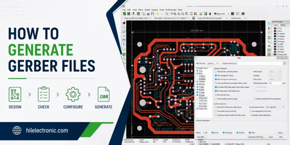
How to Generate Gerber Files for PCB Manufacturing
Figure 1. how to generate Gerber files image for Highleap...

Gerber File Review Checklist: How to Check PCB Files Before You Order
Figure 1. Gerber file review catches missing layers, drill...
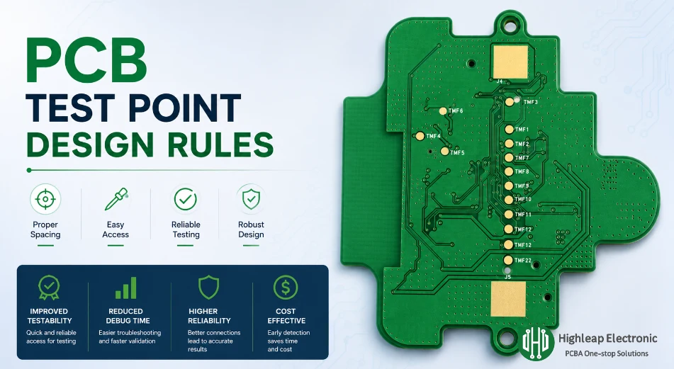
PCB Test Point Design Rules for Debug and ICT
Figure 1. PCB test point design rules help make debugging,...

PCB Jumper Wire: Uses, Types, and Design Tips
Figure 1. PCB jumper wires are useful for prototypes and...