
PCB Manufacturing Process Flow: Complete Fabrication Routes
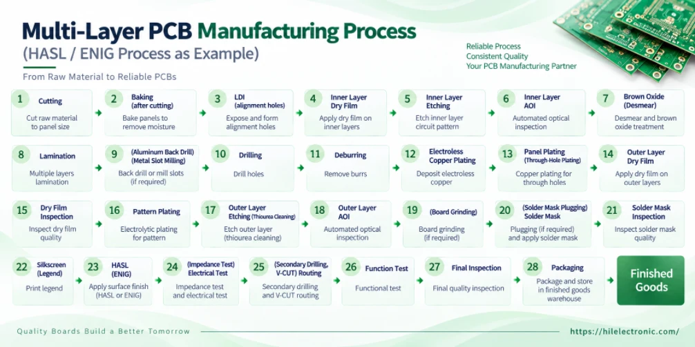
There is no single PCB manufacturing process flow that applies to every board. A double-sided plated-through-hole board, a multilayer PCB, a negative-plated board, a PTFE high-frequency board, a blind/buried-via build, and a board with mixed surface finishes can follow materially different production routes.
This page is organized as a PCB process-route library. It shows the manufacturing sequence for each major board or process type, including the conditional operations that are inserted only when the design requires them. For the engineering logic behind CAM, DFM, compensation and production-data release, see the main PCB manufacturing process guide.
Panel Cutting → Post-Cutting Bake → LDI Registration → Inner-Layer Dry Film → Inner-Layer Etching → Inner-Layer AOI → Brown Oxide → Lamination → Drilling → Deburring → Electroless Copper → Panel Plating → Outer-Layer Dry Film → Dry-Film Inspection → Pattern Plating → Outer-Layer Etching → Outer-Layer AOI → Solder Mask → Legend → Surface Finish → Electrical Test → Routing → Final Inspection → Packaging.
Optional branches such as metallized-slot routing, solder-mask via plugging, impedance testing, second drilling and V-scoring are inserted only when required.
PCB Manufacturing Process Flow Selector
| PCB / requirement | Recommended route on this page | Main process difference |
|---|---|---|
| Double-sided PTH PCB | Double-sided pattern-plating flow | No inner-layer imaging or multilayer lamination. |
| Multilayer PCB | Multilayer pattern-plating flow | Adds inner layers, AOI, brown oxide and lamination. |
| Negative-plated PCB | Negative-plating flows | Copper build occurs before negative-film imaging and negative etching. |
| Hole copper without matching surface-copper build | Selective hole-copper plating flow | Adds dedicated hole-plating film and separate copper/tin plating stages. |
| PTH + NPTH requiring separate drilling timing | PTH / NPTH split-drill flow | NPTH drilling is inserted after pattern plating and before etching. |
| Controlled-depth metallized slot | Semi-metallized controlled-depth slot flow | Through-slot and step-slot machining occur at different production stages. |
| PTFE / Rogers-type high-frequency material | PTFE plasma-treatment flows | Adds material conditioning and plasma before copper deposition; a separate pre-solder-mask conditioning step is also used. |
| Mechanical blind/buried-via build | Blind/buried-via negative-plating branch | Adds sub-board processing, copper reduction and additional plating/imaging loops. |
| Special electrical or registration verification | Special test routes | Test operations are inserted at defined checkpoints rather than at the normal final-test position. |
| Mixed surface finish / gold fingers | Surface-finish branch routes | Gold plating, masking, tape protection, HASL or other finish operations change the downstream order. |
1. Core PCB Fabrication Process Flows
These are the base production routes. Special holes, materials, finishes and tests are added as branch operations to one of these core flows.
1.1 Bare Board / Blank Panel — Direct Process Core route
- 1. Panel Cutting
- 2. Drilling
- 3. Negative Etching
- 4. Routing
- 5. Final Inspection
- 6. Packaging
- 7. Finished-Goods Warehouse
Used for simple blank-board processing that does not require the laminated single-sided route.
1.2 Bare Board / Blank Panel — Laminated Process Core route
- 1. Panel Cutting
- 2. Post-Cutting Bake
- 3. Negative Dry Film — single-side lamination and exposure
- 4. Negative Etching
- 5. Lamination
- 6. Drilling
- 7. Secondary Negative Etching
- 8. Routing
- 9. Final Inspection
- 10. Packaging
- 11. Finished-Goods Warehouse
This branch is used when the blank-board construction requires lamination. Copper must remain available before drilling in this route.
1.3 Single-Sided and Pseudo-Double-Sided PCB Core route
- 1. Use the approved single-sided manufacturing route
- 2. Drill all non-plated holes according to the released drill definition
- 3. Complete single-sided circuit formation
- 4. Apply required finish and profile operations
- 5. Final Inspection
- 6. Packaging
A double-sided layout with no metallized holes is treated as a pseudo-double-sided board and follows the single-sided route rather than the normal PTH double-sided process.
1.4 Double-Sided Pattern-Plating PCB Core route
- 1. Panel Cutting
- 2. Post-Cutting Bake
- 3. Aluminum Entry-Sheet Drillingif required
- 4. Mechanical Drilling
- 5. Metallized Slot Routingif required
- 6. Deburring
- 7. Electroless Copper
- 8. Panel Plating
- 9. Outer-Layer Dry Film
- 10. Dry-Film Inspection
- 11. Pattern Plating
- 12. Outer-Layer Etching — thiourea cleaning where specified
- 13. Outer-Layer AOI
- 14. Surface Brushing / Grindingif required
- 15. Solder-Mask Via Pluggingif required
- 16. Solder Mask
- 17. Solder-Mask Inspection
- 18. Legend / Silkscreen
- 19. HASL, ENIG or specified Surface Finish
- 20. Impedance Testif required
- 21. Electrical Test
- 22. Second Drilling / V-CUTif required
- 23. Routing
- 24. Feature Inspection
- 25. Final Inspection
- 26. Packaging
- 27. Finished-Goods Warehouse
This is the standard positive pattern-plating route for a two-layer board with metallized holes.
1.5 Multilayer Pattern-Plating PCB Core route
- 1. Panel Cutting
- 2. Post-Cutting Bake
- 3. LDI Registration
- 4. Inner-Layer Dry Film
- 5. Inner-Layer Etching
- 6. Inner-Layer AOI
- 7. Brown Oxide
- 8. Lamination
- 9. Aluminum Entry-Sheet Drillingif required
- 10. Mechanical Drilling
- 11. Metallized Slot Routingif required
- 12. Deburring
- 13. Electroless Copper
- 14. Panel Plating
- 15. Outer-Layer Dry Film
- 16. Dry-Film Inspection
- 17. Pattern Plating
- 18. Outer-Layer Etching — thiourea cleaning where specified
- 19. Outer-Layer AOI
- 20. Surface Brushing / Grindingif required
- 21. Solder-Mask Via Pluggingif required
- 22. Solder Mask
- 23. Solder-Mask Inspection
- 24. Legend / Silkscreen
- 25. HASL, ENIG or specified Surface Finish
- 26. Impedance Testif required
- 27. Electrical Test
- 28. Second Drilling / V-CUTif required
- 29. Routing
- 30. Feature Inspection
- 31. Final Inspection
- 32. Packaging
- 33. Finished-Goods Warehouse
Compared with a double-sided board, the multilayer route adds inner-layer imaging, inner-layer AOI, brown oxide and lamination before the through-hole process.
1.6 Double-Sided Negative-Plating PCB Negative plating
- 1. Panel Cutting
- 2. Post-Cutting Bake
- 3. Drilling
- 4. Deburring
- 5. Electroless Copper
- 6. Negative Plating
- 7. Post-Plating Surface Grinding
- 8. Negative Dry Film
- 9. Dry-Film Inspection
- 10. Negative Etching
- 11. Outer-Layer AOI
- 12. Surface Brushing / Grindingif required
- 13. Solder-Mask Via Pluggingif required
- 14. Solder Mask
- 15. Solder-Mask Inspection
- 16. Legend
- 17. HASL, ENIG or specified Surface Finish
- 18. Impedance Testif required
- 19. Electrical Test
- 20. Second Drilling / V-CUTif required
- 21. Routing
- 22. Feature Inspection
- 23. Final Inspection
- 24. Packaging
- 25. Finished-Goods Warehouse
This flow uses copper build before negative-film imaging and negative etching.
1.7 Multilayer Negative-Plating PCB Negative plating
- 1. Panel Cutting
- 2. Post-Cutting Bake
- 3. LDI Registration
- 4. Inner-Layer Dry Film
- 5. Inner-Layer Etching
- 6. Inner-Layer AOI
- 7. Brown Oxide
- 8. Lamination
- 9. Aluminum Entry-Sheet Drillingif required
- 10. Drilling
- 11. Metallized Slot Routingif required
- 12. Deburring
- 13. Electroless Copper
- 14. Negative Plating
- 15. Negative-Plating Surface Grinding
- 16. Negative Dry Film
- 17. Dry-Film Inspection
- 18. Negative Etching
- 19. Outer-Layer AOI
- 20. Surface Brushing / Grindingif required
- 21. Solder-Mask Via Pluggingif required
- 22. Solder Mask
- 23. Solder-Mask Inspection
- 24. Legend
- 25. HASL, ENIG or specified Surface Finish
- 26. Impedance Testif required
- 27. Electrical Test
- 28. Second Drilling / V-CUTif required
- 29. Routing
- 30. Feature Inspection
- 31. Final Inspection
- 32. Packaging
- 33. Finished-Goods Warehouse
The multilayer negative-plating route adds the complete inner-layer and lamination sequence before the negative-plating outer-layer process.
2. Hole Plating and Mechanical Branch Flows
These routes are inserted when hole copper, non-plated holes, plated slots or controlled-depth features cannot be handled by the standard drilling/plating sequence.
2.1 Selective Hole-Copper Plating — Hole Copper Without Matching Surface-Copper Build Hole plating
- 1. Drilling
- 2. Electroless Copper
- 3. Panel Plating
- 4. Hole-Plating Dry Film
- 5. Dry-Film Inspection
- 6. Selective Hole Copper Plating — copper only, no tin
- 7. Dry-Film Stripping
- 8. Post-Plating Surface Grinding
- 9. Outer-Layer Dry Film — normal outer-layer artwork
- 10. Dry-Film Inspection 1
- 11. Tin Plating — tin only, no additional copper
- 12. Outer-Layer Etching
- 13. Normal Downstream Process
This positive-process branch separates hole-copper build from the later outer-layer tin-plating/etch-resist operation.
2.2 Normal Board / Blind-Buried Sub-Board Hole-Plating Flow Hole plating
- 1. Previous Processas applicable
- 2. Laminationwhen applicable
- 3. Drilling
- 4. Desmear / Hole Cleaning
- 5. Electroless Copper
- 6. Panel Plating
- 7. Hole-Plating Dry Film
- 8. Selective Hole Copper Plating — copper only, no tin
- 9. Dry-Film Stripping
- 10. Post-Plating Surface Grinding
- 11. Inner-Layer Dry Film
- 12. Inner-Layer Etching
- 13. Normal Downstream Process
The manufacturing specification uses this negative-route branch for normal boards and blind/buried-via sub-boards that require a dedicated hole-plating cycle.
2.3 PTH + NPTH Split-Drill Flow Split drilling
- 1. Previous Process
- 2. Pattern Plating
- 3. Second Drilling — NPTH features
- 4. Dry-Film Stripping
- 5. Etching
- 6. Normal Downstream Process
This sequence keeps selected NPTH features out of the earlier metallization route by drilling them after pattern plating.
2.4 Semi-Metallized Controlled-Depth Slot Flow Controlled depth
- 1. Drilling
- 2. Through-Slot Routing
- 3. Normal PCB Processing
- 4. Pattern Plating
- 5. Dry-Film Stripping
- 6. Controlled-Depth / Step-Slot Routing
- 7. Outer-Layer Etching
- 8. Normal Downstream Process
The through slot participates in plating first; the controlled-depth machining is performed after resist stripping and before final outer-layer etching.
2.5 Metallized Slot / Edge-Plating Base Flow Metallized mechanical feature
- 1. Previous Process
- 2. Drilling
- 3. Slot / Edge Routing
- 4. Deburring
- 5. Electroless Copper
- 6. Normal Plating and Downstream Process
Metallized slots and edge-plating features must be machined before copper deposition so the exposed walls can be metallized.
2.6 Controlled-Depth Metallized Feature — Standard Branch Controlled depth
- 1. Previous Process
- 2. Lamination
- 3. Drilling
- 4. Controlled-Depth Slot Routing
- 5. Deburring
- 6. Electroless Copper
- 7. Normal Downstream Process
Used when the controlled-depth feature must be metallized after machining.
2.7 Controlled-Depth Metallized Feature — With Laser-Drilled Feature Controlled depth
- 1. Previous Process
- 2. Lamination
- 3. Drilling
- 4. Controlled-Depth Slot Routing
- 5. Deburring
- 6. Laser Drilling
- 7. Plasma Treatment
- 8. Chemical Cleaning
- 9. Electroless Copper
- 10. Normal Downstream Process
This branch inserts laser drilling and additional hole-wall preparation before electroless copper.
3. Blind/Buried-Via and Repeated-Drilling Process Flows
Complex interconnect structures can require sub-board fabrication, copper reduction, resin-plugging support operations and more than one metallized drilling cycle. For a broader overview of buildup structures, see HDI PCB manufacturing.
3.1 Multilayer Mechanical Blind/Buried-Via Negative-Plating Branch Blind / buried via
- 1. Panel Cutting
- 2. Post-Cutting Bake
- 3. Inner-Layer Dry Film
- 4. Inner-Layer Etching
- 5. Inner-Layer AOI
- 6. Brown Oxide
- 7. Lamination
- 8. Bake 1
- 9. Edge Milling
- 10. Resin / Smear Removal
- 11. Copper Reduction
- 12. Drilling
- 13. Deburring
- 14. Electroless Copper
- 15. Negative Plating
- 16. Negative-Plating Surface Grinding
- 17. Negative Dry Film
- 18. Dry-Film Inspection
- 19. Negative Etching
- 20. Normal Downstream Process
This route is used as a sub-board manufacturing branch for applicable mechanical blind/buried-via constructions.
3.2 Double-Sided / Sub-Board Negative-Plating Branch Blind / buried via
- 1. Panel Cutting
- 2. Post-Cutting Bake
- 3. Copper Reduction
- 4. Drilling
- 5. Deburring
- 6. Electroless Copper
- 7. Negative Plating
- 8. Negative-Plating Surface Grinding
- 9. Negative Dry Film
- 10. Dry-Film Inspection
- 11. Etching
- 12. Normal Downstream Process
This shorter branch is used when the sub-board does not require the multilayer inner-layer/lamination sequence.
3.3 Multiple Metallized Drilling Cycles Repeated PTH drilling
- 1. Previous Process
- 2. First Metallized Drilling Operation
- 3. Bake 1
- 4. Plasma Treatment
- 5. Glass-Fiber / Hole-Wall Treatment
- 6. Second Metallized Drilling Operation
- 7. Bake 2
- 8. Plasma Treatment 1
- 9. Glass-Fiber / Hole-Wall Treatment 1
- 10. Electroless Copper 1
- 11. Normal Downstream Process
Used when a board has more than one drilling stage and each drilling stage creates metallized through-hole features.
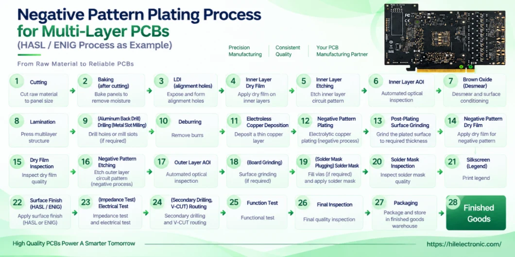
Figure 2. multi-layer-pcb-negative-pattern-plating-process-infographic
4. Material-Specific PCB Manufacturing Flows
Material selection can insert extra conditioning steps even when the circuit geometry is unchanged. The routes below show the material-specific additions defined for the corresponding material families.
4.1 PTFE High-Frequency PCB — Pre-Electroless-Copper Plasma Flow PTFE / RF
- 1. Previous Process
- 2. Drilling
- 3. Deburring
- 4. Pre-Electroless-Copper Bake
- 5. Plasma Treatment
- 6. Electroless Copper
- 7. Normal Downstream Process
Applied to applicable PTFE drilled sub-boards, PTFE/non-PTFE hybrid drilled sub-boards, mother boards and pure PTFE multilayers. For deeper material-specific manufacturing detail, see the Rogers PCB fabrication process.
4.2 PTFE High-Frequency PCB — Pre-Solder-Mask Conditioning PTFE / RF
- 1. Previous Process
- 2. Pre-Solder-Mask Bake
- 3. Solder Mask / Solder-Mask Via Plugging
- 4. Normal Downstream Process
This is a separate PTFE conditioning insertion before solder-mask processing.
4.3 N4000-Series Material Route Special material
- 1. Previous Process
- 2. Inner-Layer AOI
- 3. Brown Oxide
- 4. Post-Brown-Oxide Bake
- 5. Lamination
- 6. Drilling
- 7. Deburring
- 8. Pre-Electroless-Copper Bake
- 9. Electroless Copper
- 10. Normal Downstream Process
The material route adds thermal conditioning after brown oxide and again before electroless copper.
4.4 MEGTRON4 / FR408HR Material Route High-speed material
- 1. Previous Process
- 2. Drilling
- 3. Deburring
- 4. Pre-Electroless-Copper Bake
- 5. Plasma Treatment
- 6. Electroless Copper
- 7. Normal Downstream Process
The defined route adds both pre-copper baking and plasma treatment after drilling.
4.5 IT-150DA Material Route Dedicated material route
IT-150DA requires a material-specific manufacturing route. Confirm the exact sequence for the current stackup, hole structure and fabrication requirements during engineering release; do not assume that a standard FR-4, PTFE or MEGTRON route applies.
5. Special Test and Inspection Process Flows
These are insertion routes: the specified test is placed at a defined checkpoint rather than simply added at the end of the board.
5.1 Hole-Resistance Test Flow Special test
- 1. Previous Process
- 2. Outer-Layer AOI
- 3. Hole-Resistance Test
- 4. Solder Mask
- 5. Normal Downstream Process
Used only when hole-resistance testing is required. For standard bare-board continuity and isolation methods, see PCB electrical testing.
5.2 Inductance Test — Routing Before Electrical Test Special test
- 1. Routing
- 2. Electrical Test
- 3. Inductance Test
Used for boards whose normal route profiles the PCB before electrical testing.
5.3 Inductance Test — Electrical Test Before Routing Special test
- 1. Electrical Test
- 2. Routing
- 3. Inductance Test
Used when the product route performs electrical testing before final profiling.
5.4 Registration / Alignment Test Flow Special inspection
- 1. Previous Process
- 2. Outer-Layer Etching
- 3. Registration / Alignment Test
- 4. Outer-Layer AOI
- 5. Normal Downstream Process
Added when the customer or engineering review requires dedicated registration verification.
5.5 Controlled-Impedance Verification Position Special test
- 1. Surface Finish / Relevant Final Process
- 2. Impedance Test
- 3. Electrical Test
- 4. Normal Final Processes
Impedance testing is conditional and follows the approved coupon/test plan. See impedance-control PCB manufacturing for the design and measurement context.
6. Surface-Finish and Auxiliary Process Routes
Surface finish can move or add operations in the downstream manufacturing sequence. The flows below show the finish combinations for which the manufacturing sequence is explicitly defined. For finish selection and finish characteristics, see PCB surface finish options.
6.1 Kapton / Protective Tape Application Flow Auxiliary
- 1. Previous Process
- 2. Final Inspection
- 3. Tape Application
- 4. Second Final Inspection
- 5. Next Process
This auxiliary route is inserted where the product requires tape application before the next operation or shipment-related processing.
6.2 Lead-Free HASL — Basic Downstream Flow Surface finish
- 1. Solder Mask
- 2. Solder-Mask Inspection
- 3. Legend
- 4. Lead-Free HASL
- 5. Routing
- 6. Normal Final Processes
If legend would be printed directly over a large solder-finished area, the order may be changed so the surface finish is completed before the affected legend operation.
6.3 HASL + Gold Fingers with Plating Leads Mixed finish
- 1. Previous Process
- 2. Gold-Finger Plating
- 3. Tape Protection
- 4. Leaded or Lead-Free HASL
- 5. Normal Downstream Process
Tape protects the plated-gold region during the solder-leveling operation.
6.4 HASL + Long/Short Gold Fingers Mixed finish
- 1. Previous Process
- 2. Solder-Mask Inspection
- 3. Gold-Finger Plating
- 4. Tape Protection
- 5. Leaded or Lead-Free HASL
- 6. Normal Downstream Process
The solder-mask inspection checkpoint is completed before the plated-finger and tape-protection sequence.
6.5 Secondary Dry-Film Hard-Gold / Soft-Gold Route Electroplated gold
- 1. Previous Process
- 2. Outer-Layer Dry Film
- 3. Dry-Film Inspection
- 4. Pattern Plating
- 5. Outer-Layer Etching
- 6. Second Outer-Layer Dry Film
- 7. Second Dry-Film Inspection
- 8. Copper / Nickel / Gold Pattern Plating
- 9. Hard-Gold or Soft-Gold Electroplating
- 10. Lead Removal / Peeling where required
- 11. Normal Downstream Process
This route separates the base outer-layer circuit formation from the later selective electroplated-gold operation.
6.6 Mixed Surface-Finish Process Family Route selected by finish combination
Mixed-finish boards do not have one universal sequence. The production route is selected according to the finish combination, such as HASL + gold fingers, ENIG + selective electroplated gold, OSP + gold fingers, immersion tin + gold fingers, immersion silver + selective gold, carbon ink combinations, or peelable-mask combinations. The masking, secondary dry-film, plating, tape-protection, legend, testing and routing order must follow the finish combination actually specified for the job.
7. How to Read These PCB Process Flows
Steps marked “if required” are conditional branches rather than mandatory operations. For example, a PCB without controlled impedance does not need the impedance-test insertion, a routed board does not automatically require V-CUT, and a board without plated slots does not use the metallized-slot branch.
Likewise, a board can move from one core route into a special branch and then return to the normal downstream process. A multilayer PTFE board, for example, still has a multilayer base route, but the drilling-to-copper sequence adds the PTFE plasma-treatment branch. A PTH/NPTH design can follow the normal pattern-plating route until the second-drilling insertion is required.
Process-route principle: the finished PCB specification determines which manufacturing route is released. Layer count, plated/non-plated hole structure, copper build, material family, via construction, controlled-depth features, surface finish and special test requirements can all change the sequence.
Need a Manufacturing Route Review?
Highleap Electronics provides PCB fabrication services for standard and advanced constructions. Send the fabrication package when the board requires special hole plating, PTFE/RF materials, blind or buried vias, mixed finishes, controlled-depth machining or non-standard testing so the correct production flow can be confirmed before release.

Recommended Posts

1206 PCB Assembly Services for Prototypes & Production
src="https://hilelectronic.com/wp-content/uploads/2026/08/PC...

Kitted PCBA Services for Customer-Supplied Components
Kitted PCBA is a manufacturing model in which the customer...

Build to Print PCB Assembly Services
src="https://hilelectronic.com/wp-content/uploads/2026/08/PC...

Fine Pitch PCB Assembly Services for BGA, QFN & High-Density SMT
If you are sourcing fine pitch PCB assembly, the important...