
Back to blog
PCB Meaning: Definition, Functionality, and Applications

PCB design drawing
In the digital age, the functionality and efficiency of electronic devices hinge largely on the hidden yet crucial components they comprise. Among these, Printed Circuit Boards (PCBs) are foundational, underpinning the vast landscape of modern electronics. This article explores the pivotal role of PCBs, providing an insightful analysis of their structure, varieties, applications, and the intricate process of Printed Circuit Board Assembly (PCBA) that breathes life into these static boards.
Understanding the Backbone of Electronics: What is a PCB?
PCBs are more than just electronic placeholders; they are the platforms upon which electronic components are interconnected to form functional circuits. Traditionally known as printed wiring boards (PWBs), the evolution of PCBs reflects the convergence of circuitry and wiring into a sophisticated electronic blueprint. A PCB typically consists of multiple layers of a non-conductive substrate, primarily made from materials like fiberglass or composite epoxy, onto which conductive copper pathways are etched. These pathways serve the dual purpose of facilitating electrical connectivity and signal transmission across electronic components, making the seamless operation of devices possible.
By watching a video showcasing the fabrication process of PCBs, can gain a deeper understanding of PCB meaning
Materials Science in PCB Fabrication
Substrates
Substrates are the backbone of any PCB, providing essential structural integrity and pathways for electrical signals. Their composition significantly influences the PCB’s thermal, mechanical, and electrical properties.
FR-4
FR-4 is the industry standard for PCB substrates due to its balanced mechanical strength, moisture resistance, excellent electrical insulation, and flame retardancy. Composed of a woven fiberglass cloth with an epoxy resin binder, it is cost-effective and versatile, suitable for most low to medium performance applications. FR-4’s thermal endurance makes it compatible with the lead-free soldering required in modern environmental compliance standards.
Polyimide
For high-performance electronics that operate under extreme environmental conditions, polyimide substrates are preferred due to their ability to withstand high temperatures. This material excels in applications involving prolonged exposure to temperatures above 250°C, making it ideal for aerospace, military, and high-reliability industrial electronic products. Its flexibility also makes it suitable for dynamic applications, such as in flexible circuits.
Metal Core
Metal core substrates, including aluminum and copper, are used primarily in power electronics and LED applications where high levels of heat dissipation are required. The metal core aids in cooling by conducting heat away from critical components, thus minimizing the thermal stress on the board and enhancing the overall reliability of the system. Aluminum is more prevalent due to its cost-effectiveness and lighter weight compared to copper.
Conductive Materials: Copper
Copper is the lifeblood of PCBs, forming the critical conductive pathways that enable functionality. The choice of copper thickness impacts the board’s performance in several ways:
- Current-Carrying Capacity: Thicker copper can carry more current, making it essential for power electronics where higher current levels are involved.
- Impedance and Signal Integrity: The thickness and quality of the copper foil directly affect the impedance characteristics of the PCB. Precise impedance is crucial in high-speed digital and RF circuits to ensure signal integrity and minimize noise.
- Thermal Management: Copper’s excellent thermal conductivity also plays a role in heat dissipation. In high-power applications, thicker copper helps manage the heat generated by components, thereby reducing hot spots and improving the longevity of the device.
The copper used in PCBs typically ranges from 12 μm (1/3 oz) to 105 μm (3 oz). Selection depends on the application’s specific electrical requirements and thermal management needs. Advanced PCB designs may use varying copper thicknesses across different board areas
In summary, the materials used in PCB fabrication are chosen based on the specific requirements of the application, including thermal management, electrical performance, and mechanical durability. Innovations in material science continue to enhance the capabilities of PCBs, pushing the boundaries of what is possible in electronic design and manufacturing.

FR4 keyboard PCB in PCB
Types of PCBs
The type of Printed Circuit Board (PCB) selected for any given application depends heavily on the complexity of the circuit, the load requirements, environmental conditions, and the need for miniaturization. Here’s an in-depth look at the various types of PCBs commonly used in electronic manufacturing.
Single-sided PCBs
Single-sided PCBs are the most basic type, featuring only one layer of conductive material, typically copper, mounted on a substrate. This layer includes all the copper traces and pads which are chemically etched to create the circuit connections.
Applications
Due to their simplicity and ease of manufacturing, single-sided PCBs are the most cost-effective option and are widely used in simple electronics such as consumer gadgets, sensors, and relays. These PCBs are ideal for mass production and low-speed applications where the circuit complexity and density are minimal.
Double-sided PCBs
Double-sided PCBs have conductive copper layers on both sides of the substrate. Components can be attached to either side using through-hole or surface-mount technology, which allows for more complex circuits than can be achieved with single-sided PCBs.
Connection Techniques
- Through-hole technology: Holes are drilled through the substrate and components are mounted by inserting leads into the holes which are then soldered to pads on the opposite side.
- Surface mount technology (SMT): Components are mounted directly onto the surface of the board, allowing for more components per unit area and smaller sizes.
Applications
Double-sided PCBs are used in more complex devices where single-sided PCBs are inadequate, such as power supplies, LED lighting, automotive dashboards, and other moderate-density applications that require a compact form factor and enhanced circuitry.
Multilayer PCBs
Multilayer PCBs consist of three or more layers of conductive material interspersed with layers of insulation to separate the conductive copper layers. These layers are pressed together under high temperatures and pressures to create a single board. This configuration allows for significantly higher component density and design complexity.
Advantages
- Increased Density: Allows for more paths and more components in a smaller area, essential for modern high-density applications like smartphones and medical devices.
- Enhanced Signal Integrity: Multiple layers can be dedicated to ground and power planes, which helps in significantly reducing electromagnetic interference and improving signal integrity.
- Greater Design Flexibility: Designers can create more complex circuits without worrying about space constraints, enabling the integration of more functionality into the device.
Applications
Multilayer PCBs are crucial in advanced electronics where space, weight, and performance are critical. Typical applications include computers, telecommunications equipment, satellites, military technology, and high-performance systems where complexity and reliability are paramount.

PCB meaning, half holes board in PCB
The Process of Printed Circuit Board Assembly (PCBA)
Printed Circuit Board Assembly (PCBA) is where the theoretical design of PCBs materializes into a tangible, functional electronic device. PCBA is not merely about placing components onto a PCB; it involves several precise and methodical steps:
- Component Placement: Components are positioned according to the PCB design, using either manual placement for prototypes or automated placement for volume production.
- Soldering: After placement, components are soldered to the board, securing them in place and establishing necessary electrical connections. Techniques like wave soldering for thru-hole components and reflow soldering for surface-mount components are commonly employed.
- Inspection and Testing: Post-soldering, boards are inspected for quality assurance — often with automated optical inspection (AOI) — and tested to ensure functional integrity.

keyboard PCBA
Applications Across Industries: The Ubiquity of PCBs
PCBs are omnipresent in almost every electronic device, from simple gadgets to complex industrial systems. In consumer electronics, they are integral to the operation of smartphones, computers, and home appliances. In the medical field, PCBs are crucial for devices that require high reliability and precision, such as heart monitors and imaging equipment. The automotive industry relies on durable PCBs for engine controls, infotainment systems, and safety mechanisms, while in aerospace, they are essential for both navigation and communication systems.
Conclusion
Reflecting on the complexities and advancements discussed, it’s evident that the field of PCB manufacturing is not just maintaining pace with the technological demands of our times but is often ahead of it. As an engineer in this dynamic field, I find the continuous innovation and the challenges it brings both demanding and exhilarating. We are not just creating circuits; we are crafting the very backbone of modern technology.
In the future, as we delve deeper into realms like wearable technology and nano-electronics, the role of advanced PCB manufacturing will become even more critical. It’s an exciting time to be at the forefront of this industry, and I look forward to the new challenges and opportunities that lie ahead. This guide serves as a testament to the ingenuity and relentless pursuit of excellence within the PCB manufacturing industry, and I am proud to contribute to this ever-evolving landscape.
FQA
Q: What role do substrates play in the fabrication of PCBs?
A: Substrates provide structural integrity and pathways for electrical signals in PCBs. Their composition influences thermal, mechanical, and electrical properties.
Q: What are some advantages of using polyimide substrates in PCB fabrication?
A: Polyimide substrates excel in high-temperature environments and offer flexibility, making them ideal for aerospace, military, and industrial applications.
Q: How does copper thickness affect PCB performance?
A: Copper thickness impacts current-carrying capacity, impedance, signal integrity, and thermal management in PCBs, influencing their overall performance.
Q: What are the main techniques used in attaching components to PCBs?
A: Components can be attached using through-hole technology, where leads are inserted through holes and soldered, or surface mount technology (SMT), where components are directly mounted onto the surface of the board.
Q: In what industries are PCBs commonly used, besides consumer electronics?
A: PCBs are ubiquitous across industries such as medical, automotive, and aerospace, where they are crucial for devices ranging from medical equipment to automotive controls and navigation systems.

Related Articles
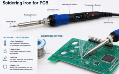
Soldering Iron for PCB: Selection Guide
Choose a soldering iron for PCB work by wattage, temperature control, tip style, and ESD safety, then use it correctly to avoid pad damage.
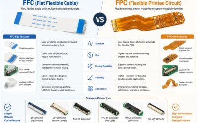
FFC vs FPC: Cable, Circuit, Connector Guide
Understand the difference between FFC and FPC interconnects, where each fits best, and how to choose compatible connectors for reliable assembly.
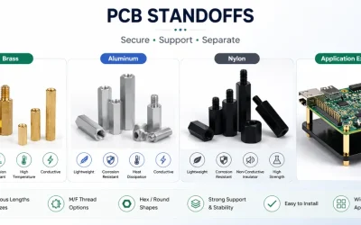
PCB Standoffs and Spacers Selection Guide
Choose PCB standoffs and spacers by material, thread size, height, and grounding needs to protect boards and simplify enclosure assembly.