
Back to blog
Selecting Your Ideal PCB Fabrication Partner in China

The electronics industry is witnessing unparalleled growth, fueled by continuous innovation and an ever-expanding demand for electronic devices. At the heart of this booming industry lies the critical role played by Printed Circuit Boards (PCBs). As the backbone of virtually all electronic products, the quality, reliability, and cost-effectiveness of PCBs are paramount. China, with its robust manufacturing ecosystem, has emerged as a global hub for PCB fabrication, offering a unique blend of technological expertise, scalability, and competitive pricing. Selecting the right PCB fabrication partner in China is a strategic decision that can significantly influence the success of your electronic projects. This guide provides a comprehensive overview of the essential factors to consider, ensuring you forge a partnership that aligns with your project’s objectives and quality standards.
Essential Factors in Choosing a PCB Fabrication Partner
Advanced Manufacturing Technologies:
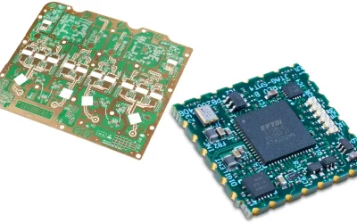
The landscape of Printed Circuit Board (PCB) fabrication is undergoing a radical transformation, driven by advancements in manufacturing technologies. These innovations not only enhance the precision and efficiency of PCB production but also open new avenues for complex designs that were previously challenging or impossible to achieve. In an era where electronic devices are becoming increasingly sophisticated, the adoption of advanced manufacturing technologies by PCB fabricators is not just a competitive edge—it’s a necessity.
Direct Imaging (DI) Technology
Direct Imaging (DI) technology uses advanced laser or LED systems to project precise circuit patterns directly onto the PCB, bypassing the need for traditional photolithography masks.
DI technology offers unparalleled precision in pattern reproduction, essential for manufacturing high-density interconnect (HDI) PCBs. It significantly reduces setup time and material costs while enhancing the speed and flexibility of the production process.
Laser Drilling
Laser drilling employs high-powered lasers to create microvias with diameters as small as a few micrometers, enabling the production of PCBs with higher circuit density and multi-layer configurations.
This technique supports the fabrication of complex PCBs for applications requiring compact sizes and high performance, such as in mobile devices and medical equipment. Laser drilling ensures clean, precise holes, improving the reliability and electrical performance of the PCB.
Automated Optical Inspection (AOI)
Automated Optical Inspection (AOI) systems utilize high-resolution cameras and sophisticated software algorithms to inspect PCBs for a wide range of defects, including missing or misplaced components, soldering faults, and trace issues.
AOI provides a rapid and accurate method for defect detection throughout the manufacturing process, significantly reducing the risk of errors and enhancing overall product quality. It is particularly crucial for ensuring the integrity of high-volume production runs.
Surface Finish Technologies
Advanced surface finish technologies, such as Electroless Nickel Immersion Gold (ENIG), Immersion Silver, and Organic Solderability Preservatives (OSP), provide a thin protective coating over the copper traces on a PCB.
These finishes enhance the solderability and corrosion resistance of the PCB, crucial for ensuring long-term reliability. They are particularly beneficial for applications requiring frequent soldering or operating in harsh environments.
Flexible PCB Production
The production of flexible PCBs (flex PCBs) involves specialized manufacturing processes that accommodate the unique properties of flexible materials, enabling the creation of bendable and foldable electronics.
Flex PCB technology is essential for modern wearable devices, medical implants, and compact consumer electronics. It offers significant advantages in terms of device miniaturization, durability, and design freedom.
Embedded Components
Embedded component technology involves integrating passive or active components directly into the PCB substrate, reducing the need for surface-mounted components.
This approach minimizes PCB size and weight while improving electrical performance by reducing signal paths. It is particularly advantageous for high-speed, high-frequency applications where space and performance are critical.
For production planning, it also helps to compare this topic with PCBA functional testing and PCB quote cost drivers before finalizing the fabrication or assembly package.
Stringent Quality Controls:
The complexity of today’s PCBs, with their finer lines, higher densities, and more sophisticated components, demands an unparalleled focus on quality at every stage of the fabrication process. Implementing rigorous quality controls ensures that each PCB meets the exacting standards required for its intended application, from simple consumer electronics to critical medical devices and aerospace systems. Here, we explore the essential elements of stringent quality controls in PCB fabrication, underlining their significance in achieving excellence.
Comprehensive Quality Management Systems (QMS)
- ISO Certifications: An ISO 9001 certification is indicative of a PCB manufacturer’s commitment to quality management principles, including a strong customer focus, the involvement of high-level company management, a process approach, and continual improvement.
- IPC Standards Compliance: Adhering to IPC standards, specifically the IPC-A-600 for PCB acceptability and IPC-A-610 for electronic assemblies, ensures that PCBs are fabricated and assembled to meet the industry’s highest quality benchmarks.
Advanced Inspection and Testing Techniques
- Automated Optical Inspection (AOI): This technology enables early detection of potential issues such as shorts, opens, insufficient solder, and component misalignment. Conducted post-soldering, AOI is crucial for ensuring the accuracy of PCB assembly.
- X-ray Inspection: Especially relevant for boards with hidden features such as buried vias or ball grid arrays (BGAs), X-ray inspection allows for non-destructive evaluation of solder joints and alignments.
- In-Circuit Testing (ICT): ICT checks for shorts, opens, resistance, capacitance, and other basic quantities to verify the functionality of assembled PCBs, ensuring they meet the specified electrical performance.
- Functional Testing: Simulating the operating environment of the PCB, functional testing ensures the board performs as intended in its final application, validating the success of the manufacturing process.
Material and Component Quality Assurance
- Raw Material Inspection: High-quality PCB fabrication begins with high-quality materials. Rigorous inspection of substrates, copper foil, and other raw materials ensures they meet the necessary specifications for purity, thickness, and durability.
- Component Verification: Ensuring the quality and authenticity of electronic components is vital to prevent failures. This includes verifying component specifications, checking for counterfeit parts, and assessing the reliability of suppliers.
Continuous Improvement and Feedback Loops
- Root Cause Analysis: Implementing a systematic approach to identifying the root causes of any detected defects allows for the effective implementation of corrective actions, reducing the likelihood of recurrence.
- Customer Feedback: Engaging with customers to gather feedback post-delivery provides valuable insights into the PCB’s performance in real-world applications, guiding continuous improvement efforts.
Competitive Pricing
Selecting a PCB manufacturer that offers competitive pricing has a direct impact on the overall cost-effectiveness and profitability of your project. It allows for better budget allocation, potentially freeing up resources that can be invested in other critical areas such as R&D, marketing, or inventory management. Furthermore, it can enhance the final product’s marketability by enabling more aggressive pricing strategies without eroding profit margins.
Lead Times and Delivery
Lead times and delivery play a critical role in the success of PCB manufacturing projects, influencing not just the production schedule but also the broader strategic objectives of electronics companies. By adopting a collaborative approach, leveraging technology, managing the supply chain effectively, and focusing on continuous improvement, businesses can optimize lead times without compromising the quality or cost-effectiveness of their PCBs. In today’s competitive market, the ability to deliver high-quality products quickly and reliably is not just an advantage; it’s a necessity.

Related Articles
Fast PCB Fabrication Manufacturer with Global Service
One-stop PCB fabrication and assembly manufacturer offering stack-up review, sourcing, SMT, and box-build—all under one roof.
PCB Projects That Perform: Design, Manufacture, and Deliver
From complex multilayer PCBs to consumer-grade designs, Highleap Electronics ensures your PCB projects succeed with trusted end-to-end service.
Reverse Engineering Circuit Boards | PCB Solutions
The goal of reverse engineering a PCB is to create a detailed schematic or layout of the board, often in the absence of the original design files or documentation.