
Castellated PCB: Essential Guide to Module Integration & DFM

Figure 1. Castellated PCB
1. Introduction: Defining the Modular Edge
A castellated PCB is a circuit board featuring half-plated holes along its perimeter, specifically engineered to enable solder-on-board module integration. These distinctive castellated edges—also called castellations or half-holes—transform sub-modules into standard SMT components that mount directly onto host boards via reflow soldering. This design approach delivers reliable electrical continuity and robust mechanical attachment between daughter modules and main assemblies.
This guide from Highleap Electronics provides the structural explanation, key DFM requirements, manufacturing process details, and reliability considerations necessary for successful castellated PCB integration in your products.
2. What Is a Castellated PCB? Structure and Terminology
2.1 Formal Definition
A castellated PCB is defined as a printed circuit board featuring half-plated holes along its edge, created by routing through the center of plated through-holes (PTHs). The resulting plated half-vias resemble the battlements of a medieval castle wall, hence the term “castellations.” Each castellation provides a solderable contact point that spans from the top copper layer to the bottom.
2.2 Fabrication Sequence
The manufacturing process follows three primary steps: Drilling → Plating → Routing/Milling. Standard PTHs are first drilled at the board edge locations, then electroplated with copper. The final routing step cuts precisely through the hole centers, exposing the plated copper and forming the characteristic semi-circular contact pads that define the castellated edge profile.
3. Why Use Castellated PCB Edges? Key Functions
3.1 SMT Module Integration and Interconnection
Castellated edges enable modules to be placed and soldered onto main boards using standard pick-and-place equipment and reflow soldering processes. The half-plated holes provide superior solder joint strength compared to simple edge pads, as the solder forms a fillet that wraps around the exposed copper barrel. This three-dimensional joint geometry ensures reliable electrical continuity and mechanical stability under operational stress.
3.2 Simplified Rework and Process Advantages
Rework Capability
Castellated modules can be removed and replaced without the complex desoldering procedures required for BGA or QFN packages. A hot air rework station easily detaches the module, and the host board pads remain intact for replacement module installation. This reduces rework time and improves yield in production environments.
Pre-Integration Testing
Module manufacturers can electrically test all key input/output connections before shipping. The exposed castellations provide accessible probe points for functional verification, ensuring defective modules are identified before integration into the final product assembly.
3.3 Compliance and Design Isolation
RF modules frequently require electrical and mechanical isolation from the host board for regulatory compliance testing and EMI shielding. Castellated PCB construction allows the module to be tested independently, certified as a standalone unit, and then integrated without re-certification of the entire assembly in many jurisdictions.

Figure 2. Castellated PCBs
4. Common Applications of Castellated PCBs
Castellated PCB modules are utilized across a wide range of electronic products. Their most common applications include:
-
Wireless communication modules such as RF, Wi-Fi, Bluetooth, and LoRa devices that rely on pre-certified radio sections to simplify development.
-
Power conversion modules including DC-DC and AC-DC converters that benefit from stable electrical interfaces and isolation from sensitive circuits.
-
Embedded system modules such as MCU cores and memory boards that extend or customize system functionality.
-
Prototyping boards including breakout boards and daughter boards that accelerate early-stage development.
Together, these applications highlight the versatility and integration efficiency of Castellated PCB technology.
5. Castellated PCB Manufacturing Process Overview
5.1 Drilling and Plating (The PTH)
The process begins with drilling standard full PTHs at designated edge locations. Copper plating thickness inside these holes is critical—insufficient plating leads to weak castellations that may fracture during routing or exhibit poor solderability. Typical specifications require minimum 20-25µm copper thickness in the barrel.
5.2 Routing or Milling (Creating the Half-Hole)
After plating and surface finishing, precision routing cuts exactly through the PTH centers. This step demands tight tolerance control to maintain consistent annular ring width on the inside of each half-hole. Routing deviation causes uneven copper exposure, leading to soldering defects or mechanical weakness in the finished castellation.
5.3 Surface Finishing
The plated half-holes receive surface finish—typically ENIG (Electroless Nickel Immersion Gold) or Immersion Tin—for optimal solderability and shelf life. ENIG provides excellent oxidation resistance and flat contact surfaces, while Immersion Tin offers cost advantages for applications with shorter storage requirements.
6. Key Design Requirements for Castellated PCBs (Critical DFM Data)
6.1 Hole Diameter and Pitch
Hole Diameter Specifications
Typical castellation hole diameters range from 0.6mm to 1.2mm. Smaller holes become difficult to plate reliably and may exhibit copper voids or thin spots. Larger holes consume additional board edge real estate. A 0.8mm to 1.0mm diameter provides optimal balance between plating quality and space efficiency for most applications.
Pitch Requirements
Minimum castellation pitch (center-to-center spacing) of 1.0mm to 1.27mm (~50 mil) is recommended. Tighter pitch risks solder bridging during reflow, while excessive spacing wastes board area. The pitch must allow proper solder fillet formation between adjacent castellations without bridging.
6.2 Annular Ring and Copper Thickness
Annular Ring Integrity
The internal copper ring must maintain sufficient width after routing to prevent copper-to-edge tear-outs. Minimum annular ring width of 0.15mm is recommended. Inadequate annular ring causes the plated copper to delaminate from the substrate during routing or under thermal stress.
Copper Plating Requirements
Adequate plating thickness ensures reliable electrical continuity from top to bottom layer through the half-hole edge. The copper barrel must withstand the mechanical stress of routing without cracking or peeling. Specify minimum 25µm plating thickness for high-reliability applications.
6.3 Solder Mask and Pad Layout
Solder Mask Clearance
Solder mask must be pulled back around each half-hole to ensure the copper is fully exposed and ready for soldering. Typical clearance of 0.1mm to 0.15mm from the castellation edge prevents mask encroachment that would inhibit solder wetting and fillet formation.
Mating Pad Design
The host PCB’s pad should extend 0.2mm to 0.3mm past the castellation edge to promote even solder wetting and adequate fillet formation. This pad extension provides additional surface area for the solder joint, improving both electrical reliability and mechanical strength of the module attachment.
6.4 Alignment and Routing Tolerance
Overall dimensional tolerance of the castellated PCB dictates reliability of the final product. High-precision routing (±0.1mm or better) is essential to prevent plating inconsistencies and ensure uniform copper exposure across all castellations. Routing misalignment causes asymmetric half-holes that exhibit inconsistent solderability and compromised mechanical strength.

Figure 3. Castellated PCB Boards
7. Castellated PCB Design Best Practices
7.1 Module Mechanical Strength
Distribute castellated holes evenly along the module edge, placing holes at corners to maximize mechanical strength of the attachment. Corner castellations resist torque and prevent module lift-off under vibration or thermal cycling stress.
7.2 Component Keep-Out Zones
Avoid placing components, vias, or critical traces within 1.0mm of the castellation edge. The routing process can induce mechanical stress that damages nearby features. Maintaining adequate clearance also prevents contamination of the castellated edge during component soldering.
7.3 SMT Alignment Features
Include fiducial markers near castellated edges on the host PCB to ensure precise module placement during automated SMT assembly. Fiducials enable vision systems to accurately position pick-and-place equipment, preventing misalignment that causes solder defects or open circuits.
8. Castellated PCB Reliability and Inspection
8.1 Solder Joint Integrity
The primary failure point in castellated module assemblies is often the solder fillet. Ensure adequate solder paste volume to create a concave fillet that maximizes joint strength. Visual inspection should confirm complete wetting of the castellation copper and smooth fillet formation on the host pad.
8.2 Thermal Cycling Performance
Assess module reliability under thermal cycling to verify the half-hole structure withstands stress from CTE mismatch between module and host board. The solder joints must accommodate differential expansion without cracking or delamination over the product lifecycle.
8.3 Panelization Considerations
When panelizing castellated modules, ensure the routing path for singulation does not introduce excessive vibration that could damage the fragile half-hole copper plating. Controlled-depth routing or proper fixturing minimizes stress during panel separation.
9. Comparison: Castellated PCB vs. Standard Edge Pads
| Aspect | Castellated PCB | Standard Edge Pads |
|---|---|---|
| Mechanical Strength | Strong 3D solder joints with high stability. | Weak flat-pad joints suitable for low-stress use. |
| Electrical Reliability | Robust electrical connection with better solder wetting. | Limited reliability; best for light-duty interfaces. |
| SMT Integration | Well-suited for standard reflow assembly. | Less secure during reflow; not ideal for permanent mounting. |
| Reworkability | Easier module replacement and repair. | Less favorable due to weaker joints. |
| Manufacturing Complexity | More complex and slightly higher cost. | Simple and low-cost. |
| Typical Use Cases | Permanent, high-reliability modules. | Temporary or low-power connections. |
10. Summary
Castellated PCBs represent the gold standard for high-reliability, solderable module integration, enabling SMT assembly of sub-circuits as standard components. Success depends on strict adherence to DFM rules—particularly hole diameter, pitch specifications, and precise routing tolerances that ensure clean, strong plating along the cut edge.

Recommended Posts

High Speed PCB Material Selection for Signal Integrity
Figure 1. High speed PCB material selection. On this page...
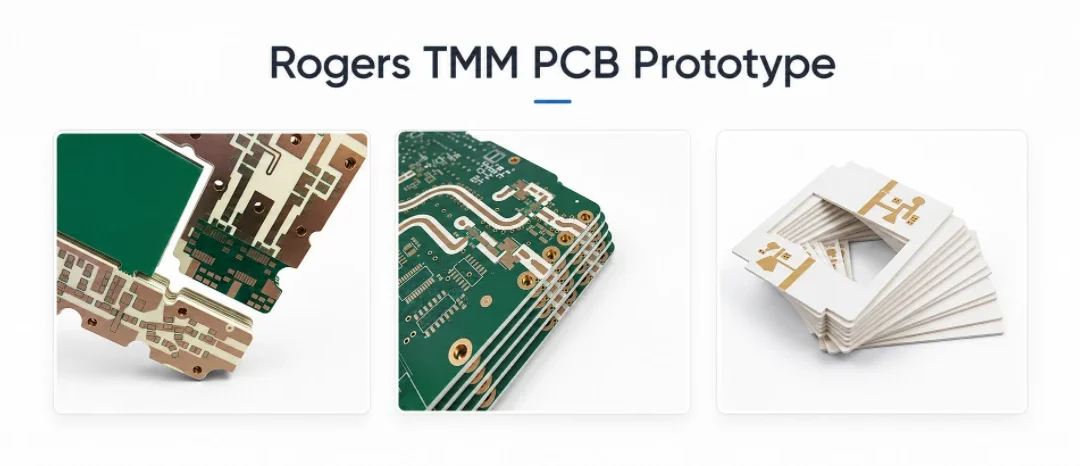
Rogers TMM PCB Prototype Manufacturing for RF Validation and Pre-Production
Table of Contents Rogers TMM PCB Prototype Manufacturing...
Rogers TMM Antenna PCB Manufacturing for Patch, Array and mmWave Designs
Table of Contents Rogers TMM Antenna PCB Manufacturing for...
Rogers TMM RF PCB Design and Manufacturing for Controlled Impedance
Table of Contents Rogers TMM RF PCB Design and...
How to get a quote for PCBs
Let‘s run DFM/DFA analysis for you and get back to you with a report. You can upload your files securely through our website. We require the following information in order to give you a quote:
-
- Gerber, ODB++, or .pcb, spec.
- BOM list if you require assembly
- Quantity
- Turn time
In addition to PCB manufacturing, we offer a comprehensive range of electronic services, including PCB design, PCBA, and turnkey solutions. Whether you need help with prototyping, design verification, component sourcing, or mass production, we provide end-to-end support to ensure your project’s success.
For PCBA services, please provide your BOM (Bill of Materials) and any specific assembly instructions. We also offer DFM/DFA analysis to optimize your designs for manufacturability and assembly, ensuring a smooth production process.