
LGA Package: Structure, Benefits, and PCB Design Guide

Figure 1. LGA Package
1. Introduction: Why LGA Package Matters in Modern Electronics
The demand for higher I/O counts, faster signal speeds, and improved thermal management continues to drive semiconductor packaging innovation. Traditional packages like QFP face limitations in pin density and signal integrity at high frequencies, while BGA packages, though effective, introduce challenges related to solder joint inspection and rework.
The Land Grid Array (LGA) package addresses these constraints through a fundamentally different approach: flat metal contact pads on the package underside, eliminating protruding pins or solder balls. This design enables connection via socket pressure or direct PCB soldering, offering engineers flexibility in high-performance applications.
This article examines LGA package structure, benefits, limitations, PCB design implications, and application scenarios.
2. What Is an LGA Package?
2.1 LGA Package Definition
LGA stands for Land Grid Array. Unlike packages with protruding leads or attached solder balls, an LGA package features an array of flat metallic pads (lands) on its bottom surface. Electrical connection occurs through one of two methods: mechanical pressure from an LGA socket with spring-loaded contacts, or direct soldering to corresponding PCB pads. The absence of ball or pin structures on the component itself transfers connection complexity to the socket or board assembly.
2.2 How LGA Differs from PGA and BGA
The distinction lies in where the interconnect structure resides. Pin Grid Array (PGA) packages have pins attached to the component that insert into socket holes. Ball Grid Array (BGA) packages carry solder balls that reflow onto PCB pads during assembly. LGA packages shift this paradigm: all raised contact structures exist on the socket or PCB side, leaving the package with only flat pads. This architectural difference impacts assembly methods, replacement procedures, and thermal interface options.

Figure 2. LGA and BGA and PGA
3. LGA Package Structure and Components
3.1 Bottom Contact Pads
The underside of an LGA package presents a dense array of metallic pads, typically finished with nickel/gold (Ni/Au) plating for oxidation resistance and reliable contact. These pads are arranged in a grid pattern with pitch values often below 1mm. Unlike BGA packages where solder balls provide self-alignment during reflow, LGA pads require precise mechanical positioning since no self-centering mechanism exists during assembly.
3.2 Substrate and Internal Interconnects
Above the contact array sits the package substrate, constructed from organic laminate or ceramic material depending on performance requirements. The die attaches to this substrate through wire bonding or flip-chip interconnection. High-performance LGA packages typically use flip-chip technology for shorter signal paths and better electrical characteristics. The substrate routes signals from the die to the external contact pads through multiple internal layers.
3.3 Socket System Architecture
In socket-based applications, the LGA socket forms a critical system component. Spring-loaded contacts within the socket press against the package lands when a retention mechanism applies load. This mechanism typically includes a load plate and lever system that distributes force evenly across all contacts. Socket quality directly determines contact resistance, long-term reliability, and maximum operational cycles.

Figure 2. LGA Package Sideview
4. Advantages of LGA Package Technology
4.1 Superior I/O Density
Without solder balls occupying vertical space, LGA packages achieve tighter pad pitches and higher I/O counts within equivalent footprints. This density advantage proves essential for modern processors and ASICs requiring thousands of connections. Engineers can implement more functionality in constrained board areas while maintaining signal routing flexibility.
4.2 Enhanced Electrical Performance
The LGA package structure minimizes parasitic inductance by eliminating ball or pin length from the signal path. Shorter interconnects translate to reduced impedance discontinuities and improved signal integrity at high frequencies. For applications demanding low jitter and clean signal edges, this electrical advantage directly impacts system performance margins.
4.3 Thermal and Mechanical Benefits
LGA packages allow direct heatsink attachment to the package lid without intermediate structures compromising thermal transfer. The socket-based connection distributes mechanical stress evenly, reducing localized strain that causes solder joint fatigue in BGA assemblies. This configuration improves long-term reliability under thermal cycling conditions.
4.4 Component Replaceability
Socket-mounted LGA packages enable chip replacement without soldering or desoldering operations. This capability proves valuable in development environments, server platforms requiring field upgrades, and test systems where component swapping occurs frequently. The non-destructive replacement process reduces maintenance time and eliminates rework-induced board damage.

Figure 3. Land Grid Array
5. Challenges and Limitations of LGA Packages
5.1 Assembly Alignment Requirements
LGA packages lack the self-alignment characteristic that solder surface tension provides in BGA assembly. Placement accuracy depends entirely on pick-and-place equipment precision and PCB pad positioning. Coplanarity requirements for both the package and board become more stringent, as uneven surfaces result in open contacts.
5.2 Socket Cost and Complexity
High-quality LGA sockets with reliable spring contacts represent significant BOM cost additions. These sockets occupy board real estate beyond the package footprint and add assembly steps. For cost-sensitive applications or space-constrained designs, socket overhead may outweigh replaceability benefits.
5.3 Direct Solder Challenges
When LGA packages are soldered directly to PCBs rather than socketed, the process window narrows considerably. Solder paste volume, stencil aperture design, and reflow profile control require tighter tolerances than equivalent BGA processes. Inspection also becomes more difficult, as X-ray imaging of flat pad joints offers less definitive assessment than ball-shaped connections.
5.4 Contamination Sensitivity
The flat contact surfaces of LGA packages are susceptible to dust, oxidation, and handling contamination. Unlike solder joints that form metallurgical bonds, pressure contacts require clean surfaces for low-resistance connections. Assembly environments and storage conditions demand stricter contamination controls compared to permanently soldered packages.
6. PCB Design and Assembly Considerations for LGA Packages
6.1 PCB Pad Design Requirements
LGA pad layouts require precise dimensional control matching package specifications. Surface finish selection affects contact reliability, with ENIG (Electroless Nickel Immersion Gold) being the predominant choice for its flat, solderable, and oxidation-resistant properties. Pad coplanarity across the footprint must remain within tight tolerances to ensure all contacts engage properly under socket pressure.
6.2 Assembly Process Controls
For soldered LGA applications, solder paste deposition requires consistent volume and coverage across all pads. Stencil thickness and aperture geometry directly impact joint formation. Reflow profiles must accommodate the thermal mass of LGA packages while maintaining appropriate time-above-liquidus windows. Post-reflow inspection relies heavily on X-ray systems, as visual inspection cannot assess hidden pad connections.
6.3 Comparison with BGA Assembly
While BGA assembly benefits from solder ball self-alignment and consistent joint geometry, LGA assembly depends more heavily on mechanical placement accuracy. BGA inspection can assess ball collapse and shape through X-ray, whereas LGA joints present flatter profiles with less distinguishable features. These differences require adjusted process validation approaches and inspection criteria for LGA implementations.
7. Typical Applications for LGA Packages
LGA package technology finds primary use in applications demanding high performance and potential field upgradeability.
-
High-end CPUs and GPUs – High I/O density and efficient thermal paths support performance-intensive desktop and server platforms.
-
Data center processors – Socketed LGA packages enable processor upgrades and hardware refresh without full board replacement.
-
Network processors and communication ASICs – Low parasitic effects and short interconnects support multi-gigabit signal integrity.
-
Industrial control systems – Socket-based LGA designs provide flexibility for development, validation, and long lifecycle support.
-
Automated test equipment (ATE) – Component interchangeability and repeatable contact performance simplify testing and maintenance workflows.
Overall, LGA packages are favored in systems where high I/O density, electrical performance, and serviceability justify the added socket and assembly complexity.
8. LGA Package Selection Criteria
Engineering decisions regarding LGA package adoption should evaluate several factors.
-
I/O count and density requirements – Determine whether LGA’s high-density interconnect advantages justify added design and assembly complexity.
-
Signal frequency and integrity targets – Assess whether shorter interconnect paths deliver measurable performance benefits at the intended data rates.
-
System lifecycle and upgrade strategy – Evaluate the need for field replaceability when choosing between socketed and direct-solder LGA implementations.
-
Manufacturing capability and tolerances – Confirm that PCB fabrication precision and assembly processes can reliably support LGA requirements.
-
Total cost considerations – Balance socket costs, tighter process controls, and potential yield impacts against performance and serviceability gains.
LGA package selection is a trade-off decision that must align electrical, mechanical, manufacturing, and lifecycle priorities at the system level.
9. Conclusion: LGA Package Value and Application Boundaries
LGA package technology represents a targeted solution for high-density, high-performance semiconductor applications where I/O requirements, signal integrity, and component serviceability drive design choices.
The flat-pad architecture offers genuine advantages in electrical performance and thermal management while enabling non-destructive component replacement in socket configurations. However, these benefits come with increased assembly precision requirements, higher socket costs, and narrower process windows for direct-solder implementations.
LGA is not inherently superior to BGA or other package types—rather, it serves specific engineering requirements where its characteristics align with system objectives. Successful adoption depends on matching LGA capabilities to application demands, manufacturing capabilities, and lifecycle requirements.

Recommended Posts
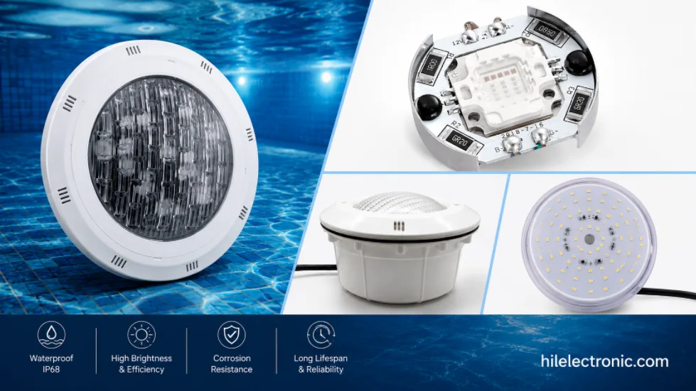
Underwater & Pool LED Light PCBs: IP68 Potted Boards, Low-Voltage Drivers & Safety
Figure 1. LED pool light PCB manufacturing reference....
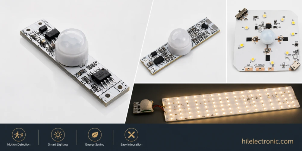
Motion Sensor & Smart LED Light PCBs: Sensor, Control, Driver & Wireless Boards
Figure 1. motion sensor LED light PCB manufacturing...
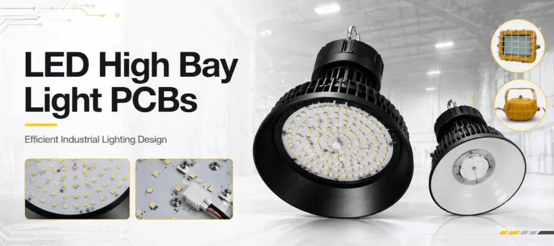
LED High Bay Light PCBs: Metal-Core Light Engines, Drivers & Turnkey Boards Built to Spec
Figure 1. LED high bay light PCB manufacturing reference....
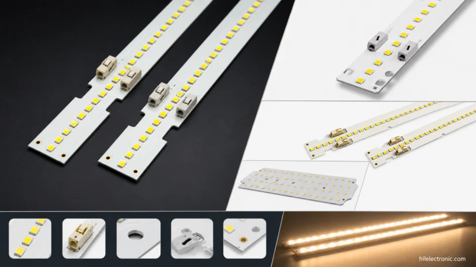
LED Linear & Strip Light PCBs: Long-Format Engines, Flexible & Rigid-Flex Boards
Figure 1. LED linear light PCB manufacturing reference....
How to get a quote for PCBs
Let‘s run DFM/DFA analysis for you and get back to you with a report. You can upload your files securely through our website. We require the following information in order to give you a quote:
-
- Gerber, ODB++, or .pcb, spec.
- BOM list if you require assembly
- Quantity
- Turn time
In addition to PCB manufacturing, we offer a comprehensive range of electronic services, including PCB design, PCBA, and turnkey solutions. Whether you need help with prototyping, design verification, component sourcing, or mass production, we provide end-to-end support to ensure your project’s success.
For PCBA services, please provide your BOM (Bill of Materials) and any specific assembly instructions. We also offer DFM/DFA analysis to optimize your designs for manufacturability and assembly, ensuring a smooth production process.