
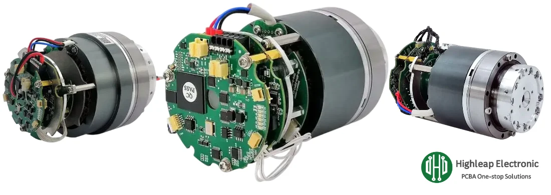
Robot Joint Driver PCB Assembly for Servo Motion

A robot joint driver is a mixed-signal power system: fast-switching power stages, sensitive feedback loops, safety-critical protection, and high-current interconnects packed into a constrained thermal volume. That combination makes robot joint driver PCB assembly unusually sensitive to manufacturing variation. A design can run fine on a bench build yet fail in production due to MOSFET voiding, inconsistent ground impedance, encoder noise pickup, connector fatigue, or uncontrolled component alternates.
This guide focuses on build specifications that scale—from prototype to volume—covering power stage assembly controls, sensing integrity, EMI/thermal risk drivers, and production validation. For programs that need a single manufacturing loop from bare boards to finished electronics, teams typically align requirements across PCB fabrication and PCBA assembly to reduce iteration cycles and performance drift.
Table of Contents
- Joint Driver PCBA Fundamentals: What Defines a Stable Build
- Power Stage Assembly: Switching Loops, Thermal Pads, and High Current
- Feedback & I/O: Encoder, Current Sense, Safety Signals, and Comms
- DFM for EMI & Thermal: What Prevents Field Noise and Overheat
- Validation and End-of-Line Test: What to Measure and Log
- RFQ Checklist + Peripheral Products: From Driver to Full Box Build
1. Joint Driver PCBA Fundamentals: What Defines a Stable Build
Robot joint drivers typically integrate: a gate driver + power devices (MOSFET/IGBT), current/voltage sensing, MCU/FPGA control, braking logic, communications (CAN/RS-485/EtherCAT), and safety protection (UVLO/OCP/OTP). Production stability comes from controlling the interfaces between these blocks—especially where power switching interacts with sensing and communication.
- Repeatable impedance of the power return path: Small changes in ground and power return impedance can translate to torque ripple, comms errors, or encoder jitter. Assembly must preserve the intended return path continuity.
- Thermal path consistency: Junction temperature margin is often set by assembly outcomes (voiding, wetting, TIM contact). For joint drivers, thermal drift can change current sense offset and protection timing.
- Mechanical robustness under motion: Vibration, cable pull, and repeated service can crack solder joints on heavy connectors, busbars, and large capacitors unless mechanical support is designed and assembled consistently.
- Controlled substitutions: “Footprint-compatible” alternates can break control loop stability, noise behavior, or reliability (e.g., shunt resistor TCR, driver propagation delay, capacitor ESR/ESL).
When the program includes sourcing plus assembly, turnkey PCBA services can simplify change control by keeping BOM decisions, process controls, and test requirements in one workflow.
2. Power Stage Assembly: Switching Loops, Thermal Pads, and High Current
The power stage is where most production escapes originate: solder voiding under power packages, marginal wetting on thick copper, and inconsistent loop inductance due to assembly variance. The objective is not just “good solder joints,” but joints that remain stable under thermal cycling and high di/dt switching.
- Thermal pad soldering and void control: QFN/DFN power stages and large exposed pads require stencil aperture tuning and reflow profiling to balance wetting with void minimization. In joint drivers, voiding is not only a thermal issue—local hotspots can increase dead-time sensitivity and current ripple.
- High-current joint integrity: DC bus inputs, phase outputs, and shunt connections should define acceptance expectations for fillet, wetting, and reinforcement. Consider mechanical anchoring for connectors exposed to cable loads.
- Switching loop repeatability: Assembly-induced variation (component height, solder volume, copper wetting) can alter parasitics and EMI. Keep critical loops compact by design and avoid “assembly-dependent” return paths.
- Isolation and creepage readiness: If the joint driver includes isolation barriers, define cleanliness, coating intent, and keepouts so creepage/clearance remains valid after assembly and cleaning.

3. Feedback & I/O: Encoder, Current Sense, Safety Signals, and Comms
Robot joint performance depends on clean sensing and deterministic interfaces. Many “firmware bugs” in production are actually assembly-driven noise injection: encoder lines contaminated by switching edges, current sense offsets from solder/thermal drift, or intermittent I/O due to connector stress.
- Encoder and resolver interfaces: Differential routing discipline only works if assembly preserves reference continuity and connector grounding. Define ESD protection placement and connector pin mapping clearly to avoid rework-induced damage.
- Current sensing integrity: Shunt resistor placement, Kelvin connections, and solder joint consistency matter. Define which nets are true Kelvin sense lines and ensure they are not “optimized away” during layout edits.
- Safety I/O robustness: STO-like signals, enable chains, and fault outputs should have stable pull networks and defined connector retention. Assembly should include strain relief and controlled hand-solder rules if required.
- Communications stability: CAN/RS-485/EtherCAT PHY behavior can degrade with ground bounce and poor shielding contact. Define connector shells, chassis bonding intent, and any common-mode choke orientation checks.
4. DFM for EMI & Thermal: What Prevents Field Noise and Overheat
A joint driver’s worst field failures are often “soft” failures: intermittent comms, random faults, position jitter, or thermal trips that happen only under load and motion. These are strongly influenced by EMI and thermal DFM—areas where manufacturing variance can either be absorbed or amplified.
- EMI-sensitive assembly points: Gate driver loops, bootstrap networks, and snubbers are sensitive to placement accuracy and solder consistency. Define polarity/orientation checks and avoid layouts that become unstable when solder volume varies.
- Copper balance and warpage control: Uneven copper distribution can warp boards, stressing BGAs/QFNs and connectors. Warpage also changes heatsink contact pressure and TIM thickness in module builds.
- Coating and contamination strategy: If you require conformal coating for humidity or contamination, define the masked areas, thickness expectations, and inspection method. Coating can improve reliability but can also worsen connector contact if applied incorrectly.
- Inspection scope by risk zone: Target inspection where it matters most—power device solder joints, hidden pads, and fine-pitch control components. A structured approach is easier to scale using comprehensive inspection coverage rather than ad-hoc checks.
5. Validation and End-of-Line Test: What to Measure and Log
Functional validation is the fastest way to prevent expensive field debugging. For robot joint drivers, “power-on OK” is not enough—tests must detect defects that only appear under load, temperature rise, or high switching activity. Production-grade testing should be designed to isolate failures quickly and generate useful logs.
- Electrical sanity checks: rail sequencing, UVLO thresholds, gate drive health, current sense offsets, and protection responses (OCP/OTP) at controlled conditions.
- Load and thermal screening: run controlled load profiles that emulate startup torque, speed ramps, braking, and sustained current. Monitor temperature rise and current regulation stability.
- Noise and comms robustness: verify encoder signal quality and error counts during switching activity; validate comms under worst-case current edges.
- Serialization and traceable logs: record test results by unit so production escapes can be contained quickly. If your product requires auditability, align build records using PCB/PCBA traceability.
For fixture planning, scripts, and scalable coverage, many teams formalize requirements using PCBA functional testing (FCT) so test limits and reporting remain consistent across volume ramps.
6. RFQ Checklist + Peripheral Products: From Driver to Full Box Build
High-quality RFQs get high-quality quotes. Joint drivers are complex, so quoting and DFM are fastest when your package states build intent, risk zones, and test expectations. The same manufacturing line often supports adjacent robotics electronics, enabling you to consolidate suppliers if desired.
RFQ Package Checklist (Driver PCBA)
- Design data: Gerber/ODB++, assembly drawings, net classes (power vs sensing vs comms), and any controlled clearance/isolation notes.
- BOM rules: identify no-substitute parts (shunts, gate driver ICs, isolated DC/DC, PHYs, precision references), and define alternate approval flow.
- Mechanical interfaces: connector part numbers, cable direction constraints, heatsink/TIM requirements, mounting torque notes, and any potting/coating requirements.
- Test intent: what must be verified (protection thresholds, current regulation, comms, encoder validity), the load profile, and what data must be logged per unit.
Peripheral Products Commonly Built Around Joint Drivers
- Power distribution and protection boards: DC bus boards, pre-charge circuits, e-fuse modules, and current/voltage monitoring boards.
- Encoder and sensor interface boards: resolver-to-digital modules, encoder buffer boards, IMU/force sensor interface boards, and safety I/O expanders.
- Communication and gateway modules: CAN-to-Ethernet, EtherCAT nodes, isolated RS-485 hubs, and diagnostic dongles.
- Brake and actuator accessories: brake driver boards, clutch control modules, and auxiliary motor driver boards for grippers or small axes.
- System integration assemblies: wiring harness integration, enclosure mounting, labeling, and final product assembly using box build assembly when you need a finished module rather than a bare PCBA.
If you want to start with a clean handoff, you can submit your package via Get a Quick Quote with your files, BOM rules, and test intent so the response includes actionable DFM feedback rather than generic pricing.
Summary: A production-ready Robot Joint Driver PCB Assembly program is defined by stable power-stage soldering, noise-resilient feedback interfaces, EMI/thermal DFM that absorbs manufacturing variance, and end-of-line validation under realistic load profiles. When requirements are explicit and testable, you reduce rework, prevent intermittent field failures, and scale faster with predictable lot-to-lot performance.

Recommended Posts
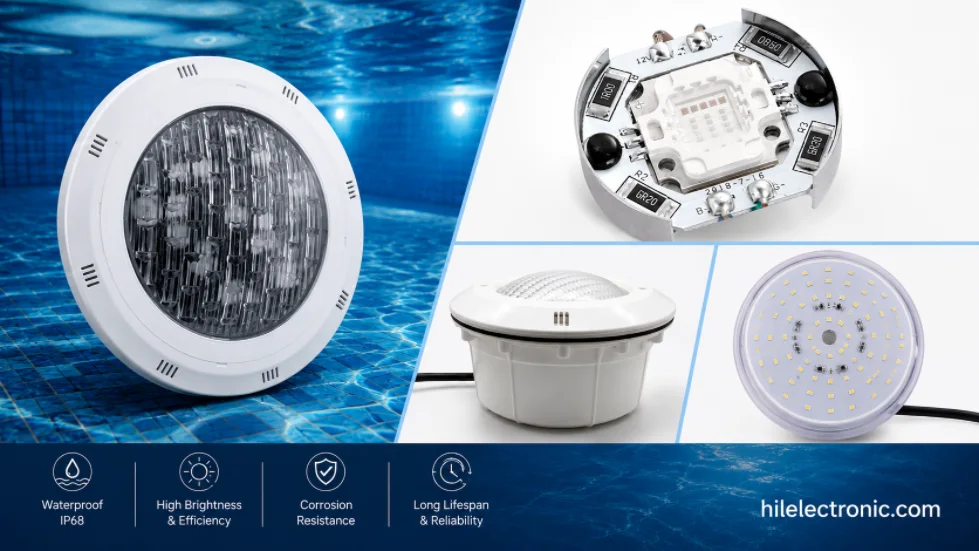
Underwater & Pool LED Light PCBs: IP68 Potted Boards, Low-Voltage Drivers & Safety
Figure 1. LED pool light PCB manufacturing reference....
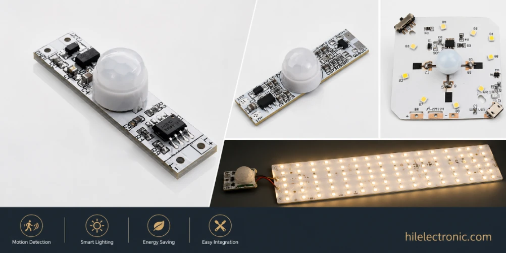
Motion Sensor & Smart LED Light PCBs: Sensor, Control, Driver & Wireless Boards
Figure 1. motion sensor LED light PCB manufacturing...

LED High Bay Light PCBs: Metal-Core Light Engines, Drivers & Turnkey Boards Built to Spec
Figure 1. LED high bay light PCB manufacturing reference....
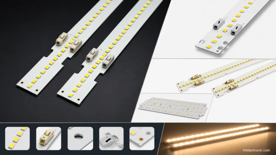
LED Linear & Strip Light PCBs: Long-Format Engines, Flexible & Rigid-Flex Boards
Figure 1. LED linear light PCB manufacturing reference....
How to get a quote for PCBs
Let us run DFM/DFA analysis for you and get back to you with a report.
You can upload your files securely through our website.
We require the following information in order to give you a quote:
-
- Gerber, ODB++, or .pcb, spec.
- BOM list if you require assembly
- Quantity
- Turn time
In addition to PCB manufacturing, we offer a comprehensive range of electronic services, including PCB design, PCBA (Printed Circuit Board Assembly), and turnkey solutions. Whether you need help with prototyping, design verification, component sourcing, or mass production, we provide end-to-end support to ensure your project’s success. For PCBA services, please provide your BOM (Bill of Materials) and any specific assembly instructions. We also offer DFM/DFA analysis to optimize your designs for manufacturability and assembly, ensuring a smooth production process.