
High-Power PCB Design and Manufacturing

High-power PCB design requires the electrical, thermal, mechanical, and manufacturing decisions to work together. Current density, voltage spacing, heat flow, component mounting, and test coverage all influence whether a board performs reliably in its end application.
This guide outlines the practical controls that make high-power PCB fabrication and assembly easier to validate and repeat.
Table of contents
- Define the Power Requirements
- Current Paths and Copper Design
- Thermal Management
- Materials, Creepage, and Clearance
- High-Power PCB Assembly Considerations
- Inspection and Validation
- High-Power PCB Support With Highleap
Define the Power Requirements
Document the continuous and peak current, voltage range, switching frequency, fault conditions, ambient temperature, cooling method, and expected duty cycle. These inputs determine conductor sizing, spacing, material selection, component derating, and the test plan.
Do not size the PCB only from average load. Startup, short-duration overloads, and abnormal operating conditions can set the real thermal and electrical limits.
Current Paths and Copper Design
Trace width, copper thickness, via count, connector rating, and solder-joint geometry all affect current capacity. Map the full current loop, including returns, to identify bottlenecks rather than focusing on one visibly wide trace.
Where heavy copper or parallel paths are needed, confirm etching tolerances and assembly clearances with the manufacturer during DFM review.
Thermal Management
Heat must move from the source into copper, vias, thermal interface materials, heat sinks, enclosure features, or airflow. Use thermal analysis and measurement to find hot spots around power semiconductors, inductors, resistors, and connectors.
Thermal vias and copper pours are useful only when there is a complete path to a cooler structure. Keep temperature-sensitive components away from concentrated heat sources where possible.

Materials, Creepage, and Clearance
Select laminate, dielectric thickness, solder mask, and surface finish from the electrical environment and assembly process. Creepage and clearance requirements depend on voltage, pollution degree, coating, altitude, and applicable product standards.
Document the required rules in the layout and drawing package so that routing changes or panelization do not compromise them later.
High-Power PCB Assembly Considerations
High thermal mass areas need a soldering process that achieves reliable wetting without overheating nearby components. Component placement, stencil design, reflow profile, selective soldering, and mechanical support should be reviewed as one assembly system.
Large terminals and heavy parts may require additional mechanical retention. Their pads, drill sizes, and solder fillets should be evaluated for vibration and service loading.
Inspection and Validation
Inspection should verify polarity, solder quality, critical isolation distances, and the quality of high-current joints. Functional testing can include load testing, thermal measurement, insulation checks, and fault-response evaluation appropriate to the product.
Production acceptance limits should be documented so the same criteria are applied to pilot and repeat builds.
High-Power PCB Support With Highleap
Highleap Electronics can review high-power PCB data for fabrication and assembly risks before production. Providing current paths, thermal targets, stack-up requirements, and test expectations allows for a more useful manufacturing review.
For a manufacturability review, request a PCB quote with the Gerber files, BOM, drawings, and power requirements.
Get a Free PCB & PCBA Quote

Recommended Posts
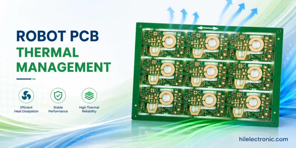
Robot PCB Thermal Management for Motors, Power Rails and Compute
Robot PCB thermal management affects service life, field...
Robot PCB EMI/EMC Design for Reliable Robotics
Robot PCB EMI and EMC design affects whether a robot can...
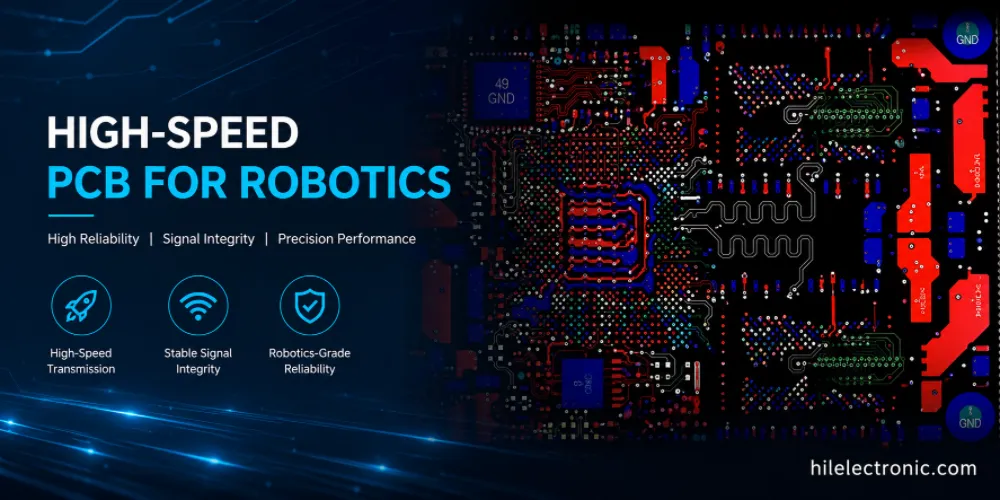
High-Speed PCB for Robotics: PCIe, DDR, MIPI and Ethernet Layout
High-speed PCB manufacturing for robotics supports data...
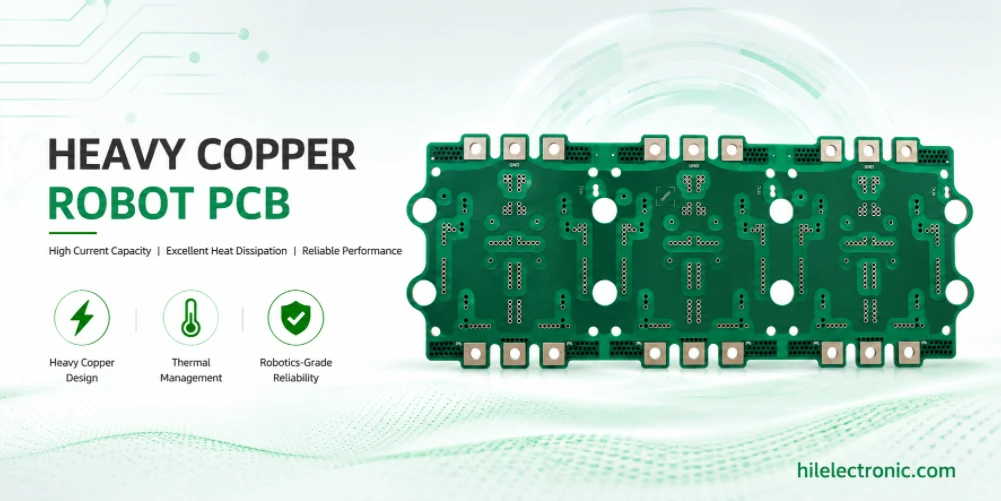
Heavy Copper Robot PCB for Motor Drives, BMS and Power Distribution
Heavy copper robot PCBs are used when standard 1 oz copper...
How to get a quote for PCBs
Let us run DFM/DFA analysis for you and get back to you with a report.
You can upload your files securely through our website.
We require the following information in order to give you a quote:
-
- Gerber, ODB++, or .pcb, spec.
- BOM list if you require assembly
- Quantity
- Turn time
In addition to PCB manufacturing, we offer a comprehensive range of electronic services, including PCB design, PCBA (Printed Circuit Board Assembly), and turnkey solutions. Whether you need help with prototyping, design verification, component sourcing, or mass production, we provide end-to-end support to ensure your project’s success. For PCBA services, please provide your BOM (Bill of Materials) and any specific assembly instructions. We also offer DFM/DFA analysis to optimize your designs for manufacturability and assembly, ensuring a smooth production process.