
Ceramic Base PCB Manufacturing & SMT Assembly Services

Table of Contents
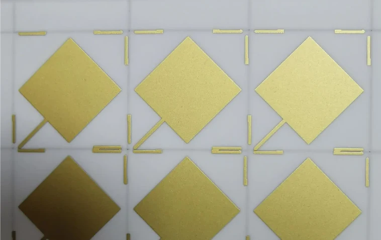
A ceramic base PCB uses alumina (Al₂O₃), aluminum nitride (AlN), or silicon nitride (Si₃N₄) as both the mechanical base and electrical insulator — no dielectric layer between the copper circuit and the mounting surface. Thermal resistance ranges from 0.3°C/W (AlN DBC) to 0.8°C/W (alumina DBC), compared to 3°C/W for aluminum MCPCB and 15°C/W for FR4.
This guide focuses on what comes after material selection: thermal stack integration, substrate thickness, surface finish, failure modes, assembly, and specification writing.
Key Takeaways
- The ceramic base is one layer in a thermal stack — substrate, TIM, and cold plate must be co-optimized
- 0.635 mm is the production standard; thinner substrates improve thermal performance but reduce handling tolerance
- Surface finish drives SMT yield and wire bondability — ENIG for SMT, hard gold when wire bonding is required
- Most field failures trace to three root causes: mounting-induced cracking, DBC delamination, and edge chipping
- A complete specification requires 12 parameters — the two most commonly omitted are bottom surface finish and isolation test voltage
1) Ceramic Base PCB in the Thermal Stack
The ceramic substrate is not a standalone thermal solution. It is one layer in a stack that runs from the device junction to the coolant — and the layers above and below it directly affect system thermal resistance.
A 50 µm silicone TIM pad at 3 W/m·K adds 0.5–1.0°C/W on top of a 0.3°C/W AlN DBC board, nearly doubling total impedance. In many systems, switching from silicone TIM to a phase-change material recovers more junction temperature than upgrading from alumina to AlN.
Three specification decisions that affect the whole stack:
- Bottom copper coverage: Full-coverage bottom copper minimizes spreading resistance at the ceramic-to-TIM interface. Partial coverage creates thermal dead zones regardless of substrate material.
- Bottom copper flatness: ≤25 µm TIR enables thin, high-conductivity TIM (phase-change, solder, silver sinter). This single spec can shift TIM conductivity from 3 W/m·K to 150+ W/m·K.
- Substrate thickness: Thinner reduces vertical conduction resistance but also reduces lateral spreading. For large-die devices, thinner is always better. For small die on large substrate, model before deciding.
2) Substrate Thickness Selection
Thickness controls two things simultaneously: thermal resistance (thinner = better) and mechanical robustness (thicker = stronger). The default 0.635 mm is right for most applications — but not all.
| Thickness | Use When | Avoid When |
|---|---|---|
| 0.25–0.32 mm | Small format (<15×15 mm), permanently bonded to a metal carrier; laser diode sub-mounts | Any application requiring manual handling, screw mounting, or boards >20 mm unsupported |
| 0.38 mm | Medium format (15–40 mm) modules bonded to baseplates; tight thermal budgets with controlled handling | Clamp-style or press-fit attachment; high-vibration environments without rigid bonding |
| 0.635 mm | Production standard for DBC power modules; screw mounting with metal bushings; general assembly handling | Permanently bonded applications where 0.38 mm would recover meaningful thermal margin |
| 1.0 mm+ | Large format (>60 mm); frequent handling during production; heavy cantilevered components | Thermal-critical applications — added conduction resistance is rarely justified on thermal grounds alone |
One constraint overrides thermal optimization: isolation voltage. At 17 kV/mm dielectric strength, a 0.635 mm alumina substrate provides approximately 10 kV working isolation. Applications requiring >10 kV cannot use thinner substrates regardless of the thermal budget.
3) Surface Finish Options
Surface finish determines solderability, wire bondability, and shelf life. It must be specified for top and bottom surfaces independently — and must match the full assembly sequence, not just the first operation.
| Finish | Structure | Best For | Not Suitable For |
|---|---|---|---|
| ENIG | 3–6 µm Ni / 0.05–0.1 µm Au | SMT assembly; lead-free solder; most production ceramic base PCBs | Wire bonding — thin Au layer causes bond lift-off |
| Hard Gold | 3–5 µm Ni / 0.5–2.0 µm Au (electroplated) | Wire bonding (Al wedge, Au ball); connector contacts; hybrid packages | Au thickness >1.5 µm can cause solder dewetting — verify with assembly process |
| Bare Copper / OSP | As-etched or organic preservative | Solder or silver sinter attach to cold plate; cost-sensitive immediate assembly | Wire bonding; multiple reflow cycles; long shelf life without hermetic packaging |
| Immersion Silver | 0.1–0.3 µm Ag | RF/microwave circuits where surface conductivity reduces insertion loss above 1 GHz | Uncontrolled storage environments — sulfur tarnish degrades solderability |
When both SMT and wire bonding are required on the same board, specify hard gold across all pads. Zonal finishing (ENIG on SMT pads, hard gold on bond pads) costs more in process complexity than the gold savings justify.
4) Field Failure Modes
Ceramic base PCB failures are mechanical and interfacial — not chemical or moisture-related like FR4. All three major failure modes are design-preventable.
Mounting-induced cracking is the most common field failure. Bare screw mounting without metal bushings applies point loads that alumina (fracture toughness 3–4 MPa·m½) cannot sustain. Fix: brazed or epoxy-bonded metal bushings at all screw locations; torque limit 0.3–0.5 N·m for M3 through aluminum bushings in 0.635 mm alumina. Adhesive attachment to the cold plate eliminates mounting point loads entirely.
DBC delamination under thermal cycling occurs when bond quality is marginal or copper geometry creates stress concentrations. Large isolated copper islands with abrupt edges are higher risk. Fix: avoid copper patch aspect ratios >5:1; specify minimum bond peel strength ≥20 N/cm²; require thermal shock testing to JEDEC JESD22-A104 at first-article qualification.
Edge chipping and crack propagation begins with handling damage — a micro-crack introduced during singulation or a dropped board. The crack is invisible at inspection but propagates to an open circuit under thermal cycling. Fix: chamfered corners (radius ≥0.3 mm); ≥0.5 mm copper-to-edge clearance; fluorescent crack detection for high-reliability lots.
Die-attach solder fatigue affects silicon dies soldered to alumina — CTE mismatch of ~3.5 ppm/°C creates shear stress that exhausts SAC305 joints within 1,000–3,000 automotive thermal cycles. Fix: use AlN substrates for GaN/SiC devices (CTE mismatch ~1.1 ppm/°C); specify silver sintering for automotive die-attach — sintered silver survives 10,000+ cycles at ΔT = 150°C; require ≤5% void fraction by X-ray.
5) Assembly and Integration
Standard FR4 assembly parameters will damage ceramic substrates. The differences are not optional adjustments — they prevent cracking and joint failures that are difficult to diagnose after the fact.
Reflow profile: Reduce ramp rate to 1–2°C/s (vs. 3°C/s for FR4). Extend the soak zone at 150–180°C to 90–120 seconds to equalize temperature across the ceramic before entering reflow. Peak temperature and time-above-liquidus remain unchanged.
Die-attach options by reliability requirement:
- SAC305 solder: Standard for non-automotive applications; ≤10% void fraction by X-ray; suitable for <3,000 cycles at ΔT ≤ 100°C
- AuSn / AuGe eutectic: Hermetic packages and high-temperature applications; requires gold-finished pads; higher joint stiffness than silver sinter
- Silver sintering: Best for automotive and aerospace; 150–250 W/m·K joint conductivity; no remelting risk in subsequent operations; requires bare copper or Ag finish on die-attach pads
Electrical interconnect — press-fit connectors cannot be used on ceramic. Standard options: soldered pin headers; edge connectors with spring contacts; ribbon/flex cable bonding; direct surface-mount to system PCB (treat the ceramic module as a component, design thermal pad and solder volume for ceramic mass and CTE).
Cold plate attachment, lowest to highest thermal resistance: solder/braze → silver sinter → phase-change TIM with clamp → thermal grease with screw clamp.
6) How to Write a Complete Specification
Incomplete specifications are the primary cause of quoting delays and first-article failures — not manufacturing capability. A ceramic base PCB RFQ requires these 12 parameters, all of them:
- Substrate material and purity — Al₂O₃ 96%, Al₂O₃ 99.6%, AlN, or Si₃N₄
- Substrate thickness ± tolerance — e.g., 0.635 mm ± 0.05 mm
- Metallization process — DBC, thick film, thin film, or AMB
- Copper thickness, top and bottom — specified independently; e.g., 0.3 mm / 0.3 mm for DBC
- Surface finish, top and bottom — most commonly omitted; bottom finish must match cold plate attachment method
- Board dimensions and tolerances — include corner chamfer or radius if required
- Minimum trace width and space — confirm against manufacturer capability before finalizing layout
- Via requirements — diameter, fill material, finish
- Electrical test requirements — continuity/isolation voltage; hi-pot voltage if required; second most commonly omitted field
- Qualification requirements — thermal cycling range and cycles; bond strength; applicable standard (AEC-Q101, IEC 60068-2-14, MIL-PRF-38534)
- Quantity breakdown — prototype and production may run on different lines with different pricing and lead times
- Layer stackup (multi-layer designs) — ceramic and conductor layer sequence; via fill and cap for LTCC or co-fired
DFM Review Before Submission
A complete specification on paper can still contain incompatible parameter combinations — for example, 100 µm trace/space on a 0.25 mm DBC substrate. Highleap Electronics provides DFM review as part of the quoting process. Our team reviews Gerber data and the full specification before quoting, confirming process capability and identifying issues before any material is committed.
7) Related Products
- DBC Substrate: The most common ceramic base PCB construction for power electronics — copper bonded to ceramic at ~1,065°C. When engineers say “ceramic base PCB” for power modules, they typically mean a patterned DBC substrate.
- Thick Film Ceramic PCB: Screen-printed conductors (5–20 µm) fired at 850–1,000°C. Lower cost than DBC for moderate-current applications; enables integrated resistors and capacitors within the ceramic base.
- AMB Substrate: Active Metal Brazing uses Ag-Cu-Ti braze at 800–900°C. Stronger copper-ceramic bond than DBC; preferred for Si₃N₄ base substrates and automotive modules requiring 10,000+ thermal cycle life.
- LTCC: Multi-layer ceramic with embedded conductors and vias co-fired at 850–900°C. Used for RF modules and multi-chip packages where the ceramic base is the three-dimensional interconnect structure, not just a thermal substrate.
- IMS / Metal-Core PCB: Lower-cost alternative when the ceramic thermal budget is not required. Thermal resistance 3–5× higher than alumina DBC. The correct choice when the application thermal budget allows it.
- Ceramic Base PCB Assembly: Die attach, wire bonding, and high-temperature reflow sourced together with substrate fabrication reduces handling risk and ensures process compatibility.

Frequently Asked Questions
What is the difference between a ceramic base PCB and a DBC substrate?
DBC (Direct Bonded Copper) is a metallization method — copper foil bonded to ceramic at ~1,065°C. All DBC substrates are ceramic base PCBs, but ceramic base PCBs also include thick film and thin film constructions. In power electronics the two terms are often used interchangeably; in RF applications, thin film on ceramic base is more common than DBC.
Can a ceramic base PCB directly replace a metal-core PCB?
Not without redesign. Ceramic requires metal bushings at mounting holes, slower reflow ramp rates (1–2°C/s), no press-fit connectors, and different singulation rules. The thermal gain is real — 0.3–0.8°C/W vs. 3°C/W for aluminum MCPCB — but the swap requires explicit changes to mounting, interconnect, and assembly process.
What surface finish is needed for both SMT and wire bonding?
Hard gold (3–5 µm Ni / 0.5–2.0 µm Au electroplated) is required. ENIG’s ~0.05 µm gold layer is too thin for wire bonding and produces bond lift-off failures. Specify hard gold across all pads when both SMT and wire bonding are in the assembly sequence.
Why do ceramic base PCBs crack after passing incoming inspection?
Most post-inspection cracking comes from assembly process, not substrate defects: bare screw mounting, over-torqued fasteners, or uneven cold plate surfaces. Sub-critical micro-cracks from singulation — invisible at standard inspection — also propagate to open circuits under thermal cycling. Fluorescent crack detection at incoming and metal bushing mounting prevent both failure modes.
What is the lead time for ceramic base PCB prototypes?
Alumina DBC: 2–4 weeks. AlN DBC: 3–5 weeks. Thick film: 3–4 weeks. Thin film: 4–6 weeks. Custom dimensions add 1–2 weeks. Providing all 12 specification parameters at RFQ eliminates the most common source of delay.
Is ceramic base PCB the same as high-temperature PCB?
No. High-temperature PCB covers ceramic, PTFE/glass, polyimide, and metal-core substrates — any board rated above FR4’s 130–150°C limit. Ceramic base is the highest-performing category: operating temperatures above 300°C, thermal conductivity 60–600× higher than polymer dielectrics. PTFE is high-temperature but offers no thermal conductivity advantage.

Recommended Posts

Wireless Mechanical Keyboard PCB Manufacturing
Table of contentsWireless Keyboard PCB Procurement...

Split Keyboard PCB Manufacturing & Assembly
Table of contentsSplit Keyboard PCBA Procurement...
Rapid Trigger Keyboard PCB Manufacturing & PCBA
Table of contentsRapid Trigger PCBA Buying and Performance...
QMK/VIA Keyboard PCB Manufacturing & Assembly
Table of contentsQMK/VIA Keyboard PCB Buying...
How to get a quote for PCBs
Let us run DFM/DFA analysis for you and get back to you with a report.
You can upload your files securely through our website.
We require the following information in order to give you a quote:
-
- Gerber, ODB++, or .pcb, spec.
- BOM list if you require assembly
- Quantity
- Turn time