
High-Frequency Ceramic PCBs for 5G, Radar & Antenna Modules

Why High-Frequency Ceramic PCBs Are Essential for Modern RF Systems
The rapid expansion of 5G infrastructure, automotive radar systems, and advanced antenna modules demands printed circuit boards capable of maintaining signal integrity at frequencies well beyond traditional applications. High-frequency ceramic PCBs leverage materials such as aluminum nitride, alumina, and silicon nitride to deliver superior electrical performance, thermal management, and dimensional stability compared to conventional polymer-based alternatives. These specialized substrates excel when applications require simultaneous management of high power density and low signal loss at frequencies exceeding 10 GHz.
While PTFE-based laminates offer excellent dielectric properties, ceramic substrates provide thermal conductivity values ten to twenty times higher, making them indispensable for active RF components where heat dissipation directly impacts reliability. The trade-off involves higher material costs and more complex manufacturing processes, which must be weighed against the performance requirements of each specific application.
Understanding High-Frequency Performance Requirements
Frequency Thresholds for Ceramic PCBs
High-frequency operation typically begins where conventional PCB materials show measurable degradation in electrical performance, generally above 1 GHz. For high-frequency ceramic PCBs, the relevant frequency spectrum spans from low microwave bands around 2 GHz through millimeter-wave frequencies approaching 100 GHz. At these operating points, electromagnetic phenomena that remain negligible at lower frequencies become primary design constraints.
Critical RF Phenomena
The skin effect concentrates current flow near conductor surfaces, effectively increasing resistance as frequency rises. Dielectric losses convert signal energy into heat, while impedance discontinuities at component interfaces and trace transitions generate reflections that degrade signal quality. High-frequency ceramic PCBs address these challenges through carefully controlled dielectric properties and superior dimensional stability, enabling predictable impedance control and minimal signal attenuation.
High-Frequency Ceramic PCB Materials: Properties and Selection Criteria
Aluminum Nitride (AlN) Substrates
Aluminum nitride represents the premium choice for high-frequency ceramic PCBs requiring exceptional thermal performance. With thermal conductivity ranging from 150 to 180 W/mK, AlN substrates efficiently spread heat from power amplifiers and transmit-receive modules. The coefficient of thermal expansion closely matches silicon at approximately 4.5 ppm/°C, reducing thermal stress in die-attach applications. Dielectric properties remain stable with a dielectric constant near 8.8 and loss tangent below 0.001 at microwave frequencies.
Alumina (Al₂O₃) Substrates
Alumina substrates offer a cost-effective alternative for high-frequency ceramic PCBs where moderate thermal conductivity suffices. Standard 96% alumina provides thermal conductivity around 20-25 W/mK, while 99.6% formulations reach 30-35 W/mK. The dielectric constant typically falls between 9.5 and 10.0, with loss tangent values around 0.0002 to 0.0005 at microwave frequencies. Alumina’s mechanical robustness and mature manufacturing processes make it the workhorse material for RF modules, filters, and antenna substrates.
Silicon Nitride and Specialty Materials
Silicon nitride brings excellent mechanical strength and moderate thermal conductivity around 15-30 W/mK to specialized applications. Silicon carbide offers even higher thermal conductivity for extreme power applications, though at increased cost. These materials fill niche requirements in high-frequency ceramic PCBs but see limited deployment compared to AlN and alumina.
PTFE-Ceramic Composite Laminates
Hybrid approaches combine PTFE matrix materials with ceramic fillers to balance properties. These laminates achieve dielectric constants from 2.2 to 10.0 depending on filler content, with exceptionally low loss tangent values below 0.0009. Thermal conductivity remains lower than pure ceramic substrates, typically 0.5-1.0 W/mK, but the materials offer easier fabrication using conventional PCB processes.
Material Performance Comparison
| Material | Dielectric Constant (10 GHz) | Loss Tangent | Thermal Conductivity (W/mK) | Primary Applications |
|---|---|---|---|---|
| AlN | 8.8 | <0.001 | 150-180 | Power amplifiers, T/R modules |
| Al₂O₃ (96%) | 9.5-10.0 | 0.0002-0.0005 | 20-25 | Antenna feeds, RF filters |
| Al₂O₃ (99.6%) | 9.8-10.0 | 0.0001-0.0003 | 30-35 | Low-loss microwave circuits |
| Si₃N₄ | 7.0-8.0 | 0.0005-0.001 | 15-30 | High-reliability modules |
| PTFE-Ceramic | 2.2-10.0 | <0.0009 | 0.5-1.0 | Ultra-low-loss transmission |
Electrical Properties That Define High-Frequency Ceramic PCB Performance
Dielectric Constant and Stability
The dielectric constant determines transmission line impedance and signal propagation velocity in high-frequency ceramic PCBs. Ceramic materials maintain exceptional stability across temperature excursions, with temperature coefficients typically below 50 ppm/°C. This stability ensures that carefully designed 50-ohm transmission lines maintain impedance accuracy from initial power-up through full thermal load.
Loss Tangent and Signal Integrity
Loss tangent quantifies the energy dissipated within the dielectric during each signal cycle. High-frequency ceramic PCBs with loss tangent values below 0.001 enable low-attenuation transmission lines essential for millimeter-wave systems. A microstrip line on alumina with 0.0003 loss tangent exhibits approximately 0.05 dB per wavelength of dielectric loss at 10 GHz.
Impedance Control Methods
Controlled impedance in high-frequency ceramic PCBs depends on precise relationships between trace geometry, dielectric thickness, and material properties. Microstrip configurations place signal traces on the top surface with a ground plane below, offering accessible routing but higher radiation at millimeter-wave frequencies. Stripline embeds traces between ground planes, providing better shielding at the cost of more complex via transitions.
Thermal Management in High-Frequency Ceramic PCBs
Heat Dissipation Capabilities
High-frequency ceramic PCBs excel in applications where RF power amplifiers, active antenna arrays, or transmit-receive modules generate significant heat flux. Aluminum nitride substrates spread heat laterally across the board while conducting through-thickness to heat sinks. A typical power amplifier die generating 10 W in a 5mm x 5mm footprint creates junction temperatures 30-40°C lower on AlN compared to alumina substrates of equivalent thickness.
Coefficient of Thermal Expansion Matching
Direct die attach requires careful attention to CTE matching between high-frequency ceramic PCBs and semiconductor materials. Silicon’s CTE of 2.6 ppm/°C matches well with AlN at 4.5 ppm/°C, generating acceptable stress levels through normal operating temperature ranges. Alumina’s 6.5-7.0 ppm/°C creates higher stress but remains viable for most applications with appropriate die-attach materials.
Mechanical Considerations
Ceramic substrates exhibit brittle fracture characteristics requiring attention during handling and assembly. High-frequency ceramic PCBs typically use thickness ranges from 0.25mm to 1.0mm depending on mechanical support requirements and electrical design constraints. Thinner substrates reduce via aspect ratios and enable compact designs but require careful handling procedures.
Manufacturing and Assembly of High-Frequency Ceramic PCBs
Ceramic Fabrication Processes
High-frequency ceramic PCBs utilize distinct manufacturing approaches compared to polymer laminates. Thick-film processes screen-print conductive pastes onto fired ceramic substrates, offering moderate resolution with excellent thermal characteristics. High-temperature co-fired ceramic (HTCC) co-processes metal and ceramic layers at 1600°C, enabling complex three-dimensional structures. Low-temperature co-fired ceramic (LTCC) systems fire below 1000°C, permitting silver and gold metallization with fine-line capability.
Metallization and Assembly
Copper metallization on high-frequency ceramic PCBs must achieve strong adhesion while maintaining low loss at microwave frequencies. Typical thickness ranges from 18μm to 100μm depending on current requirements and skin depth considerations. Component assembly uses standard solder reflow processes, though peak temperatures and ramp rates require adjustment for ceramic substrate thermal mass.
Design for Manufacturing
Critical specifications for high-frequency ceramic PCB fabrication include:
- Minimum feature sizes – Trace width and spacing typically 0.1mm to 0.15mm depending on metallization process.
- Via parameters – Diameter should exceed 0.2mm with aspect ratios kept below 5:1 for reliable plating.
- Metallization specs – Define conductor thickness, surface finish, and adhesion requirements explicitly.
- Panel constraints – Sizes generally remain smaller than polymer PCBs due to ceramic processing limitations.

Testing and Qualification of High-Frequency Ceramic PCBs
RF Characterization
S-parameter measurements from vector network analyzers provide comprehensive characterization of high-frequency ceramic PCBs. Insertion loss quantifies signal attenuation through transmission lines or assembled circuits, while return loss reveals impedance discontinuities and matching quality. Time-domain reflectometry identifies specific locations of impedance variations, enabling correlation between physical features and electrical performance.
Reliability Testing
Thermal cycling from -55°C to +125°C over 500 to 1000 cycles verifies solder joint integrity and metallization adhesion on high-frequency ceramic PCBs. Vibration testing per MIL-STD-810 confirms mechanical attachment adequacy for mobile or airborne applications. Cross-sectional analysis of via structures and component interfaces reveals potential delamination or cracking before field deployment.
High-Frequency Ceramic PCBs vs Alternative Materials
| Property | Ceramic (AlN/Al₂O₃) | PTFE-Based | Hydrocarbon Laminate |
|---|---|---|---|
| Loss Tangent (10 GHz) | 0.0001-0.001 | 0.0009-0.002 | 0.002-0.004 |
| Dk Stability (temp) | ±50 ppm/°C | ±50-200 ppm/°C | ±100-300 ppm/°C |
| Thermal Conductivity | 20-180 W/mK | 0.2-0.7 W/mK | 0.3-0.8 W/mK |
| Relative Cost | High | Medium | Low |
| Fabrication Complexity | High | Medium | Low |
Applications of High-Frequency Ceramic PCBs
5G Front-End Modules
Millimeter-wave frequencies in 5G systems demand tight control over dielectric constant to maintain phase coherence across antenna arrays. High-frequency ceramic PCBs enable integration of phase shifters, amplifiers, and radiating elements on single substrates with thermal conductivity sufficient for continuous transmission. Array configurations benefit from LTCC multilayer capability for compact three-dimensional power distribution networks.
Radar and T/R Modules
Automotive and aerospace radar systems subject RF electronics to extreme temperature ranges and vibration environments. High-frequency ceramic PCBs using alumina or AlN substrates provide mechanical robustness and thermal reliability essential for these applications. Pulsed operation creates instantaneous heat flux requiring efficient thermal spreading to avoid hot spots.
Antenna Modules and Filters
Compact filter designs exploit the high dielectric constant of ceramic materials to reduce physical dimensions while maintaining required unloaded Q factors. High-frequency ceramic PCBs enable integrated antenna implementations where radiating elements, matching networks, and active components coexist on single substrates. The thermal stability ensures consistent filter center frequency and bandwidth across operating temperature ranges.
Procurement and Manufacturer Selection for High-Frequency Ceramic PCBs
Specification of high-frequency ceramic PCBs requires clear definition of electrical, thermal, and mechanical requirements. Dielectric constant should be specified at intended operating frequency with acceptable tolerance bands. Loss tangent specification must similarly reference measurement frequency and maximum acceptable values. Substrate thickness tolerance directly impacts impedance control and should be specified tighter than standard ceramic tolerances when critical.
Manufacturing capability varies significantly among ceramic PCB suppliers. HTCC versus LTCC process selection affects available feature sizes and metallization options. Request test coupons for S-parameter characterization and cross-sectional verification before committing to full production. Qualified manufacturers should provide material certification, dimensional inspection results, and electrical test data with each lot.
Conclusion: Implementing High-Frequency Ceramic PCBs Successfully
High-frequency ceramic PCBs deliver unmatched performance for demanding RF and microwave applications where conventional materials fail to meet simultaneous electrical and thermal requirements. The combination of low dielectric loss, high thermal conductivity, and excellent dimensional stability enables reliable operation in 5G infrastructure, automotive radar, and aerospace systems.
Proper material selection between aluminum nitride and alumina depends on balancing thermal performance requirements against cost constraints. Design success requires careful attention to controlled impedance routing, ground plane architecture, and thermal management strategies specific to ceramic substrates.
Highleap Electronics High-Frequency Ceramic PCB Capabilities
Highleap Electronics provides comprehensive solutions for advanced RF applications requiring ceramic substrate technology:
- Multi-material expertise – Fabrication experience with AlN, alumina, and LTCC substrates for applications from 1 GHz to millimeter-wave frequencies.
- Precision impedance control – Controlled dielectric thickness and trace geometry to achieve ±5% impedance tolerance on critical RF transmission lines.
- Integrated assembly services – Complete turnkey solutions including die attach, wire bonding, and component assembly with thermal management optimization.
- RF testing and validation – In-house S-parameter measurement and time-domain reflectometry capabilities to verify electrical performance before delivery.
- Design support – Application engineering team provides material selection guidance, stack-up recommendations, and DFM feedback from initial concept through production.
Ready to discuss your high-frequency ceramic PCB requirements? Contact Highleap Electronics to review your specifications and receive detailed technical recommendations for your next RF project. Our engineering team specializes in translating challenging performance requirements into manufacturable, cost-effective solutions.

Recommended Posts
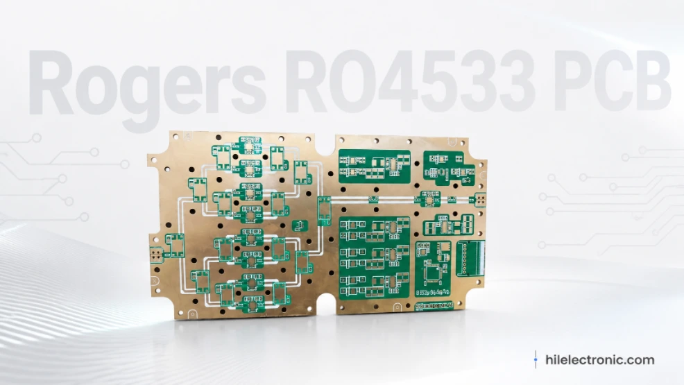
Rogers RO4533 PCB Manufacturing for Cost-Sensitive RF Products
RO4533 should be handled as a grade-specific commercial RF...
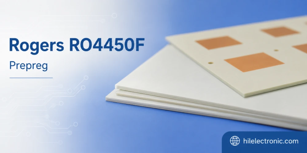
Rogers RO4450F Prepreg for Multilayer RF PCB Manufacturing
“RO4450F prepreg” is not enough information to manufacture...
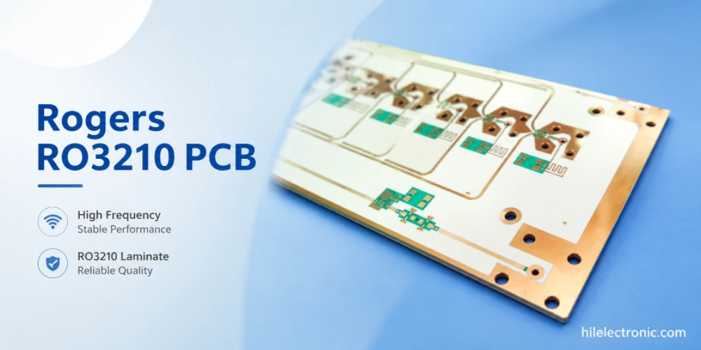
Rogers RO3210 PCB Manufacturing for Extremely Compact RF Circuits
RO3210 is not a routine material upgrade. Rogers publishes...
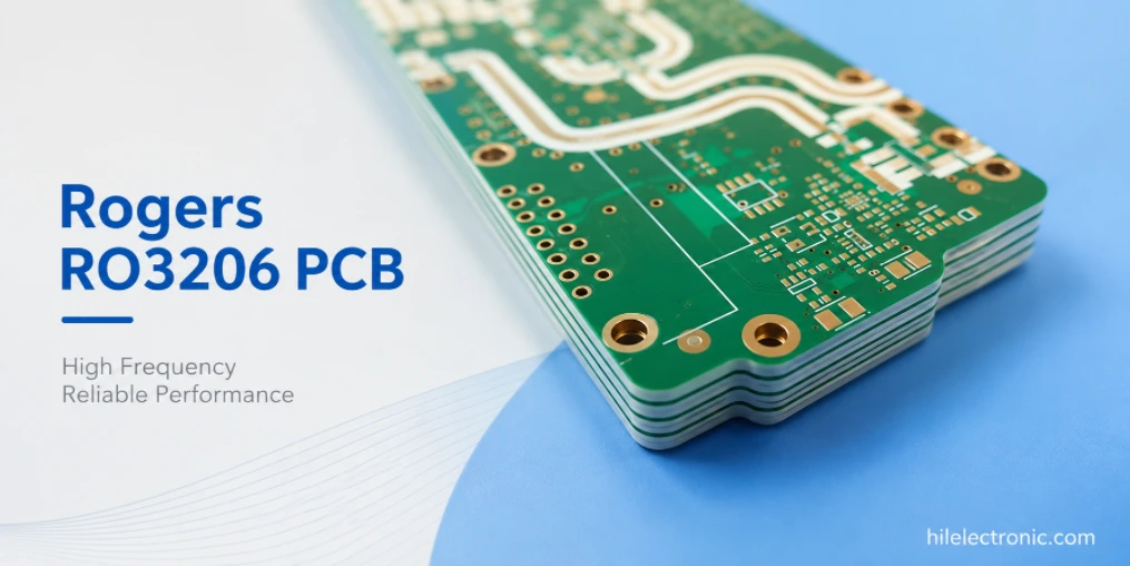
Rogers RO3206 PCB Manufacturing for Miniaturized RF Products
An RO3206 quotation should begin with the dimensions the...
How to get a quote for PCBs
Let‘s run DFM/DFA analysis for you and get back to you with a report. You can upload your files securely through our website. We require the following information in order to give you a quote:
-
- Gerber, ODB++, or .pcb, spec.
- BOM list if you require assembly
- Quantity
- Turn time
In addition to PCB manufacturing, we offer a comprehensive range of electronic services, including PCB design, PCBA, and turnkey solutions. Whether you need help with prototyping, design verification, component sourcing, or mass production, we provide end-to-end support to ensure your project’s success.
For PCBA services, please provide your BOM (Bill of Materials) and any specific assembly instructions. We also offer DFM/DFA analysis to optimize your designs for manufacturability and assembly, ensuring a smooth production process.