
MCU Clock Circuit Design: A Complete Guide to Reliable PCB Implementation

1. Introduction: The Heartbeat of Your MCU System
The MCU clock circuit design represents the fundamental heartbeat of any digital PCB, governing every aspect of system timing, data integrity, and overall reliability. When this critical subsystem fails or underperforms, the consequences cascade throughout the entire design—manifesting as system instability, excessive electromagnetic interference (EMI), degraded power efficiency, and data corruption that can compromise product quality and field reliability.
This guide delivers a systematic approach to clock source selection, essential PCB layout rules, and proven optimization techniques. Whether you are designing consumer electronics or industrial control systems, mastering MCU clock circuit design principles ensures maximum stability and performance. At Highleap Electronics, our PCB manufacturing and assembly expertise has refined these practices through thousands of production runs.
2. MCU Clock Circuit Design Fundamentals
The Role of Clock Signals
The clock signal serves as the central synchronization mechanism for all internal MCU operations. It coordinates instruction execution, manages peripheral timing (timers, UARTs, SPI, I2C), and establishes the fundamental processing speed of the system. Every state transition within the microcontroller depends on this precise timing reference.
Oscillator Basics
An oscillator converts electrical energy into stable, repetitive waveforms through controlled feedback mechanisms. In MCU applications, oscillators generate the clock frequencies that drive digital logic. The oscillator’s stability directly determines system timing accuracy and communication reliability.
Oscillator Types Overview
Internal RC/LC oscillators offer simplicity and low cost but suffer from limited accuracy and high sensitivity to temperature and supply variations. External crystal oscillators provide superior accuracy and temperature stability, making them essential for precise timing and high-speed communication protocols requiring tight frequency tolerance.
3. MCU Clock Source Selection: Critical Trade-Offs
Selecting the appropriate clock source requires balancing accuracy requirements, environmental conditions, cost constraints, and application demands. The following comparison guides clock source decisions for your MCU clock circuit design:
| Clock Source | Accuracy | Temp Stability | Cost/Complexity | Typical Use Case |
|---|---|---|---|---|
| Internal RC/LC | Low | Low | Lowest / Simple | Startup, Watchdog timers |
| Ceramic Resonator | Medium | Medium | Low | Cost-sensitive, tolerable drift |
| Crystal Oscillator | High | High | Medium / High | USB, Ethernet, RF, precision timing |
| External Clock | High | High | Medium | Multi-device synchronization |
Selection Guidance
For high-performance MCU PCB designs requiring USB, Ethernet, RF communication, or precision timing, external crystal oscillators remain the industry standard. Despite slightly increased PCB complexity, crystals deliver the frequency stability and accuracy that modern protocols demand. Internal oscillators suit only non-critical functions like watchdog timers or initial startup sequences.
4. PCB Layout Guidelines for MCU Clock Circuit Design
Critical Rule: Minimize the loop area of the oscillator circuit to reduce EMI radiation and susceptibility to external noise. This principle underlies every layout decision in MCU clock circuit design.
Component Placement
Position the crystal and load capacitors immediately adjacent to the MCU oscillator pins (OSCI/OSCO), maintaining trace lengths under 10mm. Create a tight, closed loop between the MCU pins, crystal, and load capacitors. Symmetrical placement of load capacitors relative to the crystal ensures balanced parasitic capacitance and optimal oscillation.
Routing Strategy
Keep traces between the MCU and crystal short, direct, and appropriately wide to minimize inductance. Clock traces must never run parallel to high-speed digital signals or lengthy analog lines. Maintain adequate clearance from switching power supplies and high-current paths that generate magnetic field interference.
Grounding and Guarding
Ground Plane Integrity: Maintain an uninterrupted, solid ground plane directly beneath the entire oscillator area. Never route signal traces or create ground plane splits beneath oscillator components—this introduces inductance and compromises return current paths.
Guard Ring Implementation: Surround the oscillator circuit with a dedicated copper pour connected to the ground plane. This guard ring provides electromagnetic shielding, isolates the sensitive oscillator from adjacent noisy circuits, and establishes a low-impedance boundary for stray currents.

5. Optimizing MCU Clock Circuit Design Performance
Load Capacitor Selection
Specify high-stability NP0/C0G ceramic capacitors for load capacitors to ensure frequency stability across temperature variations. These dielectric types exhibit minimal capacitance drift with temperature and voltage, unlike X7R or X5R alternatives. Calculate load capacitor values precisely using the crystal’s specified load capacitance (CL) and account for PCB parasitic capacitance (typically 3-5pF).
Power Supply Decoupling
Place dedicated low-ESR bypass capacitors immediately adjacent to MCU power pins to prevent supply noise from coupling into the oscillator circuit. A 100nF ceramic capacitor combined with a 10µF bulk capacitor provides effective broadband filtering. Route power traces to minimize the loop area between capacitor, MCU power pin, and ground.
Jitter Mitigation
Clock jitter—short-term frequency instability—directly increases bit error rate (BER) in high-speed protocols like USB and Ethernet, compromising communication reliability. The layout practices outlined in Section IV constitute the primary defense against external noise sources that induce jitter. Additional jitter reduction comes from proper power supply filtering and avoiding ground bounce near oscillator circuits.
6. MCU Clock Circuit Design Pitfalls and Solutions
Pitfall 1: Distant Crystal Placement
Positioning the crystal more than 10mm from the MCU dramatically increases noise susceptibility and EMI radiation. Long traces act as antennas, coupling interference into the clock signal and radiating emissions that may cause regulatory compliance failures.
Pitfall 2: Incorrect Load Capacitance
Mismatched load capacitor values force the crystal to operate off its specified frequency, causing timing errors and potential communication failures. Always calculate CL values accounting for both the crystal specification and PCB parasitic capacitance.
Pitfall 3: Signal Layer Conflicts
Routing high-frequency signals beneath oscillator components or traces introduces capacitive and inductive coupling that injects noise directly into the clock circuit. Reserve the area beneath the oscillator exclusively for uninterrupted ground plane.
Pitfall 4: Antenna Effects
Long, exposed clock traces behave as unintentional antennas, both radiating EMI and receiving external interference. Short, direct routing combined with guard ring shielding eliminates this common failure mode.
7. Conclusion
In MCU PCB design, the clock circuit design forms the absolute foundation of system reliability. Success depends on selecting the appropriate clock source for your application requirements and strictly adhering to DFM layout principles throughout the design process.
Prioritize solid ground plane integrity, minimum trace lengths, NP0/C0G load capacitors, and robust guard ring isolation during your initial PCB layout phase. These investments in MCU clock circuit design yield dividends in reduced EMI, improved timing accuracy, and enhanced field reliability. For expert guidance on implementing these practices in your next project, Highleap Electronics offers comprehensive PCB manufacturing and assembly services backed by decades of production experience.

Recommended Posts

RF Transceiver PCB Manufacturing and Assembly
Table of contentsRF Transceiver PCB Manufacturing and...
RFSoC Board PCB Manufacturing and Assembly One-Stop Service
Highleap Electronics supports customer-designed RFSOC...
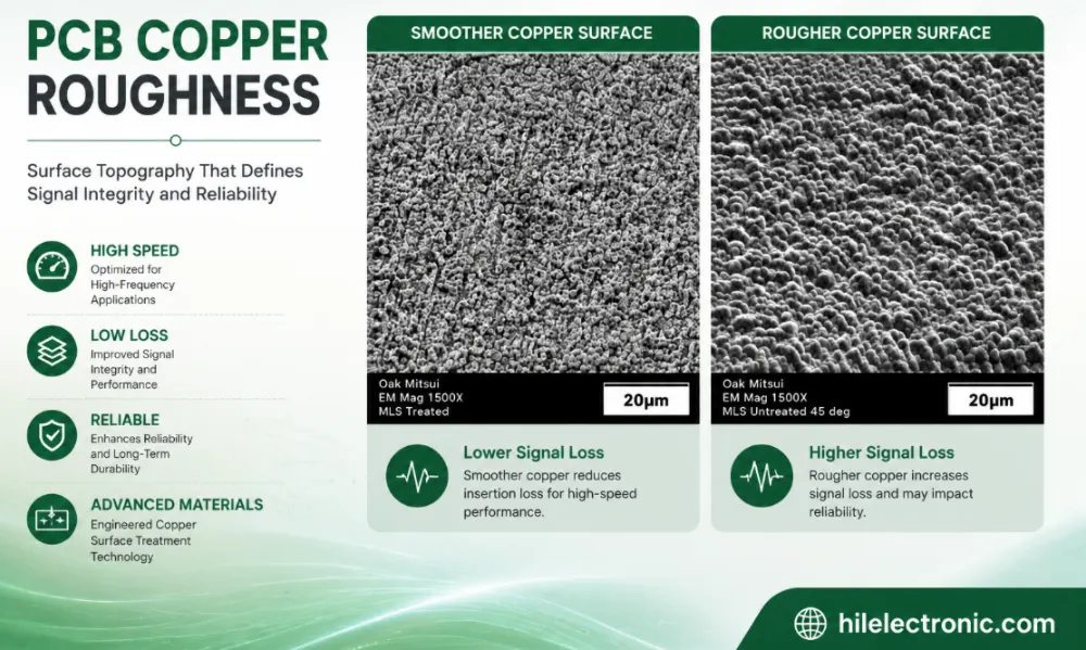
PCB Copper Roughness: Signal Loss, Material Selection and Manufacturing Control
Table of contentsWhat Is PCB Copper Roughness?How Copper...
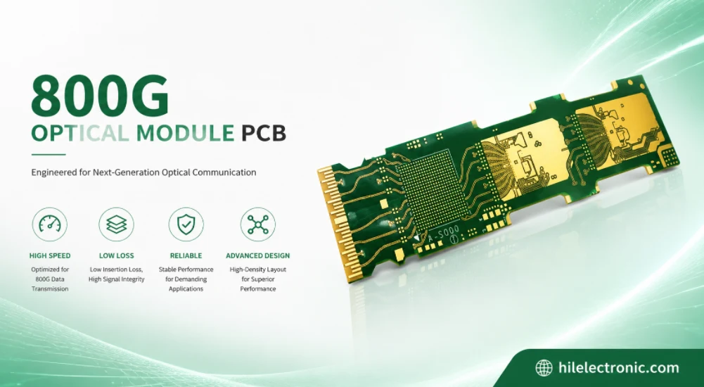
800G Optical Module PCB Manufacturing and Assembly Service
Table of contentsWhat Makes an 800G Optical Module PCB...
How to get a quote for PCBs
Let‘s run DFM/DFA analysis for you and get back to you with a report. You can upload your files securely through our website. We require the following information in order to give you a quote:
-
- Gerber, ODB++, or .pcb, spec.
- BOM list if you require assembly
- Quantity
- Turn time
In addition to PCB manufacturing, we offer a comprehensive range of electronic services, including PCB design, PCBA, and turnkey solutions. Whether you need help with prototyping, design verification, component sourcing, or mass production, we provide end-to-end support to ensure your project’s success.
For PCBA services, please provide your BOM (Bill of Materials) and any specific assembly instructions. We also offer DFM/DFA analysis to optimize your designs for manufacturability and assembly, ensuring a smooth production process.