
Multilayer Ceramic PCB: Structure, Manufacturing Process, and Applications

What is Multilayer Ceramic PCB Technology?
A multilayer ceramic PCB integrates multiple ceramic dielectric layers with internal conductor patterns to create three-dimensional circuit architectures. Unlike single-layer ceramic boards, these multilayer structures enable significantly higher circuit density and complex interconnection schemes within compact form factors. This advanced packaging approach has become essential for modern electronic systems requiring superior thermal management, high-frequency performance, and exceptional reliability.
The shift toward multilayer ceramic substrates directly responds to increasing demands from high-power electronics, millimeter-wave communications, and safety-critical automotive systems. Industries such as aerospace, radar systems, and RF communications increasingly rely on these substrates to meet stringent performance specifications where conventional organic PCBs cannot deliver adequate thermal or electrical performance.
Multilayer Ceramic PCB Structure and Key Components
Layer Composition
The fundamental building blocks of a multilayer ceramic PCB consist of alternating dielectric ceramic layers and patterned conductor layers bonded through high-temperature co-firing. Each component serves a specific function in the overall substrate performance:
- Dielectric layers – Alumina (Al₂O₃), aluminum nitride (AlN), or glass-ceramic composites selected based on thermal conductivity and dielectric requirements
- Conductor patterns – Silver, tungsten, molybdenum, or copper chosen according to firing temperature and electrical performance targets
- Via interconnections – Vertical electrical pathways connecting multiple routing layers, enabling three-dimensional circuit design
- Ground and power planes – Embedded internal layers that enhance electromagnetic shielding and reduce switching noise
Stack-Up Architecture
A typical multilayer ceramic substrate contains four to twenty layers, though specialized designs may incorporate more. Each dielectric layer ranges from 50 to 250 micrometers in thickness, allowing precise control over interlayer capacitance and characteristic impedance. Via interconnections, formed by laser drilling or mechanical punching before lamination, create the vertical electrical connections enabling complex routing across multiple planes.
Advantages Over Single-Layer Designs
While single-layer ceramic PCBs offer excellent thermal properties, multilayer ceramic boards provide exponentially greater design flexibility. The three-dimensional architecture eliminates crossing constraints, enables differential pair routing with precise spacing control, and accommodates far higher component densities. Internal ground planes provide superior electromagnetic compatibility compared to single-layer designs, making multilayer structures essential for sensitive RF and high-speed digital circuits.

Multilayer Ceramic PCB Manufacturing: LTCC and HTCC Processes
Low Temperature Co-fired Ceramic (LTCC)
LTCC technology operates at firing temperatures around 850°C, enabling highly conductive silver or gold-based metallization. This lower temperature range permits integration of embedded passive components such as capacitors and resistors directly within the ceramic layers. The result is highly integrated modules with reduced assembly complexity and improved electrical performance through shortened interconnection paths.
High Temperature Co-fired Ceramic (HTCC)
HTCC substrates undergo sintering at approximately 1600°C, necessitating refractory metal conductors like tungsten or molybdenum. The HTCC process produces ceramic structures with superior mechanical strength, higher density, and better hermeticity compared to LTCC variants. These characteristics make HTCC multilayer ceramic boards particularly suitable for harsh environment applications where mechanical robustness and long-term reliability are paramount.
Manufacturing Process Steps
The production of multilayer ceramic PCBs follows a precisely controlled sequence:
- Green tape preparation – Ceramic powder mixed with organic binders is cast into thin, flexible sheets
- Conductor printing – Screen printing applies metal pastes in precisely defined patterns onto each layer
- Via formation and filling – Holes are punched or laser-drilled and subsequently filled with conductive material
- Layer alignment and lamination – Multiple layers are carefully aligned and pressed together under controlled conditions
- Co-firing – The assembly undergoes controlled heating that burns out binders, sinters ceramic particles, and fuses conductor layers
- Post-processing – Surface metallization, solderable finishes, and precision dicing complete the fabrication

Electrical and Thermal Performance of Multilayer Ceramic PCB
Dielectric Properties
Multilayer ceramic PCB substrates exhibit dielectric constants typically ranging from 5 to 9, depending on material composition. This moderate dielectric constant enables controlled impedance design for high-frequency applications while maintaining compact circuit geometries. The low loss tangent of ceramic materials ensures minimal signal attenuation, making these substrates ideal for millimeter-wave and microwave circuits operating beyond 30 GHz.
Thermal Management Capabilities
Aluminum nitride multilayer ceramic boards deliver thermal conductivity values up to 170 W/m·K, far exceeding conventional alumina substrates and approaching copper performance. This exceptional heat spreading capability allows direct mounting of high-power semiconductor devices without intermediate thermal interface materials. Even standard alumina multilayer ceramic PCBs, with thermal conductivity around 20-30 W/m·K, outperform organic substrates by an order of magnitude.
Thermal Expansion Matching
The coefficient of thermal expansion for ceramic substrates closely matches silicon semiconductor materials at 6 to 8 ppm/°C. This thermal compatibility minimizes thermomechanical stress during temperature cycling, reducing solder joint fatigue risk in chip-on-board assemblies. The dimensional stability of multilayer ceramic boards across temperature extremes ensures consistent electrical performance from cryogenic to elevated operating temperatures.
Key Advantages of Multilayer Ceramic PCB Technology
The multilayer ceramic PCB delivers distinct performance benefits that make it indispensable for demanding applications:
- High-density interconnection – Three-dimensional architecture accommodates thousands of via connections and multiple routing layers within minimal footprints
- Superior thermal dissipation – Exceptional heat spreading enables higher power densities and improved device performance in thermal-intensive applications
- Excellent high-frequency performance – Low dielectric loss and controlled impedance characteristics support millimeter-wave circuits with minimal signal degradation
- Mechanical robustness – Ceramic substrates resist corrosion, maintain structural integrity under vibration and shock loads, and exhibit minimal degradation over extended lifetimes
- Component integration – LTCC technology enables embedded passive components, reducing assembly complexity and improving electrical performance
Design Limitations and Manufacturing Challenges
Cost Considerations
Manufacturing costs for multilayer ceramic PCBs significantly exceed those of conventional organic substrates due to specialized materials, precision processing equipment, and extended production cycles. The co-firing process requires carefully controlled atmospheres and temperature profiles, with limited opportunities for rework if defects occur. These economic factors make multilayer ceramic boards most appropriate for applications where performance requirements justify the investment.
Processing Complexity
Achieving precise layer-to-layer alignment during lamination presents technical challenges, particularly as via sizes decrease and layer counts increase. Shrinkage during firing must be accurately predicted and compensated in the initial artwork, as dimensional changes can reach 15-20 percent. The need for specialized design rules and manufacturing expertise creates barriers for companies unfamiliar with ceramic substrate technology.
Size Constraints
Panel sizes for multilayer ceramic PCB production typically remain smaller than organic PCB panels, limiting economies of scale. Large-format ceramic substrates face increased risk of warpage and cracking during firing, effectively constraining practical dimensions to smaller module formats.

Ceramic PCBs in Power Electronics and LED Applications
Multilayer Ceramic PCB Applications Across Industries
RF and Microwave Systems
RF and microwave systems extensively utilize multilayer ceramic substrates for filters, diplexers, power amplifiers, and antenna feed networks operating from UHF through millimeter-wave frequencies. The low dielectric loss and controlled impedance characteristics enable high-performance passive circuits with minimal insertion loss. Satellite communications, 5G infrastructure, and radar systems depend on these ceramic modules for reliable signal processing at frequencies exceeding 30 GHz.
Automotive Electronics
Advanced driver assistance systems and autonomous vehicle platforms require multilayer ceramic PCBs for radar transceivers operating at 24 GHz and 77 GHz frequencies. The thermal stability and reliability of ceramic substrates ensure consistent performance across automotive temperature ranges from -40°C to +150°C. Sensor fusion modules integrate multiple functions onto single multilayer ceramic boards, reducing system complexity while improving electromagnetic compatibility.
Power Electronics
High-power applications benefit from the superior heat dissipation characteristics of multilayer ceramic substrates:
- IGBT modules – Direct bonding of power semiconductors enables compact designs with improved efficiency
- DC-DC converters – Low parasitic inductances support faster switching speeds and reduced electromagnetic interference
- LED drivers – High thermal conductivity maintains junction temperatures for optimal light output and extended lifetimes
Aerospace and Medical Devices
Aerospace systems demand the reliability and hermeticity provided by HTCC multilayer ceramic boards for communication systems and sensor packages. Medical applications utilize miniaturized multilayer ceramic PCBs for implantable devices and diagnostic equipment where biocompatibility and long-term stability are critical requirements.
Conclusion
Multilayer ceramic PCB technology delivers unmatched performance for demanding electronic applications requiring high reliability, superior thermal management, and excellent high-frequency characteristics. The combination of three-dimensional routing capability, stable electrical properties, and robust mechanical structure makes these substrates essential for aerospace, automotive, and telecommunications systems.
Highleap Electronics specializes in manufacturing multilayer ceramic PCBs using both LTCC and HTCC processes, providing complete solutions from initial design consultation through prototype fabrication and volume production. Our engineering team optimizes stack-up configurations, selects appropriate materials, and ensures manufacturability for complex multilayer designs. Contact our applications engineering group to explore how multilayer ceramic substrate technology can enhance your next-generation electronic systems.

Recommended Posts
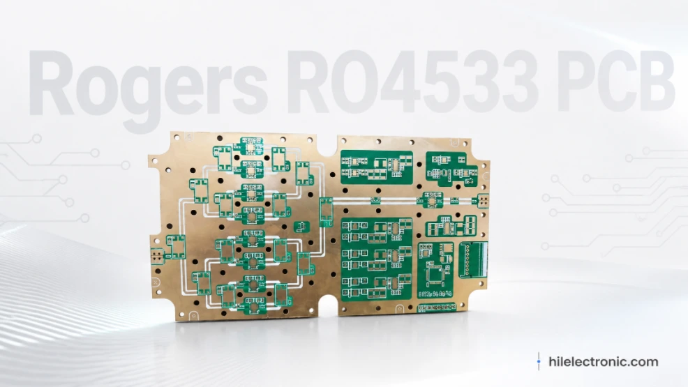
Rogers RO4533 PCB Manufacturing for Cost-Sensitive RF Products
RO4533 should be handled as a grade-specific commercial RF...
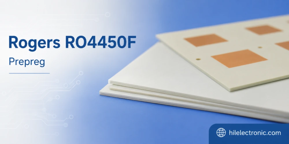
Rogers RO4450F Prepreg for Multilayer RF PCB Manufacturing
“RO4450F prepreg” is not enough information to manufacture...
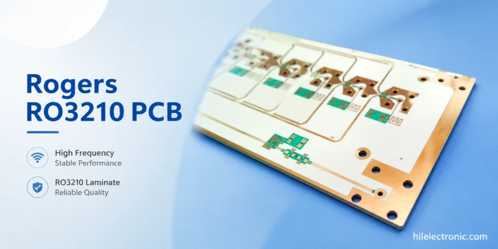
Rogers RO3210 PCB Manufacturing for Extremely Compact RF Circuits
RO3210 is not a routine material upgrade. Rogers publishes...
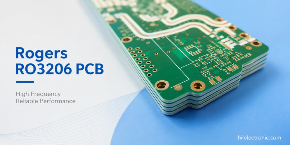
Rogers RO3206 PCB Manufacturing for Miniaturized RF Products
An RO3206 quotation should begin with the dimensions the...
How to get a quote for PCBs
Let‘s run DFM/DFA analysis for you and get back to you with a report. You can upload your files securely through our website. We require the following information in order to give you a quote:
-
- Gerber, ODB++, or .pcb, spec.
- BOM list if you require assembly
- Quantity
- Turn time
In addition to PCB manufacturing, we offer a comprehensive range of electronic services, including PCB design, PCBA, and turnkey solutions. Whether you need help with prototyping, design verification, component sourcing, or mass production, we provide end-to-end support to ensure your project’s success.
For PCBA services, please provide your BOM (Bill of Materials) and any specific assembly instructions. We also offer DFM/DFA analysis to optimize your designs for manufacturability and assembly, ensuring a smooth production process.