
SOP Package: Structure, Variants, and PCB Design Considerations

Figure 1. SOP Package
1. Introduction: What Is an SOP Package?
The SOP package (Small Outline Package) is a surface mount IC package designed for automated PCB assembly. Developed during the transition from through-hole to SMT technology, it features a flat rectangular body with dual-row gull-wing leads extending from two opposite sides. This configuration enables reliable solder joints on standard PCB pads while maintaining visual inspection capability.
The SOP package addressed a fundamental industry need: reducing board space while improving manufacturing throughput. Unlike DIP packages requiring drilled holes, SOP components mount directly on the PCB surface, enabling higher component density and double-sided assembly. This practical advantage established SOP as a foundational package type that remains relevant in modern electronics manufacturing.
2. Basic Structure and Physical Characteristics of SOP Packages
Package Body Construction
The SOP package body consists of a molded plastic enclosure (typically epoxy resin) that protects the die and wire bonds. The low-profile body—significantly thinner than DIP equivalents—enables compact product designs. Standard SOP packages accommodate 8 to 28 pins, with leads distributed equally on two parallel sides.
Lead Configuration and Pitch
SOP packages use gull-wing leads that bend outward and downward from the package body. This geometry creates accessible solder joints visible from above, facilitating both automated optical inspection and manual rework. Standard lead pitch ranges from 1.27mm (50 mil) for conventional SOP to finer pitches in shrink variants. The exposed lead design distinguishes SOP from leadless packages where connections hide beneath the component.
Comparison with Through-Hole Packaging
The SOP package eliminates the need for plated through-holes, reducing PCB layer count requirements and manufacturing cost. Surface mounting also enables shorter signal paths compared to through-hole leads, improving electrical performance in many applications. These structural advantages drove widespread SOP adoption across consumer, industrial, and automotive electronics.

Figure 2. SOP Package Structure
3. Common Types and Variants of SOP Packages
The SOP package family encompasses multiple variants optimized for different space and performance requirements. Each variant maintains the core dual-inline, gull-wing lead concept while adjusting dimensions and pitch to address specific design constraints.
Standard SOP
The original SOP format uses 1.27mm lead pitch and body widths of 3.9mm to 7.5mm depending on pin count. This configuration offers excellent manufacturability with standard SMT equipment and tolerates typical process variations. Standard SOP remains widely used for analog ICs, logic devices, and low-pin-count microcontrollers.
SSOP (Shrink Small Outline Package)
SSOP reduces lead pitch to 0.65mm or 0.635mm, enabling higher pin counts in a smaller footprint. This variant requires tighter PCB design rules and more precise placement equipment. SSOP balances space efficiency against manufacturing complexity, suitable for designs requiring moderate density increases.
TSOP (Thin Small Outline Package)
TSOP emphasizes reduced package height (typically under 1.2mm) while maintaining reasonable lead pitch. Originally developed for memory ICs in space-constrained applications like PCMCIA cards, TSOP accommodates thin product designs where vertical clearance is limited. The thinner body requires careful handling during assembly.
MSOP (Mini Small Outline Package)
MSOP combines reduced body size with fine pitch (typically 0.5mm), achieving significant area savings versus standard SOP. This variant demands high-precision SMT processes and may challenge hand rework. MSOP suits portable devices and dense PCB layouts where space optimization is critical.
4. SOP Package vs Other IC Packages
Selecting an IC package involves balancing electrical requirements, board space, manufacturing capability, and cost. The SOP package occupies a specific position in this trade-off space, distinct from both legacy through-hole formats and modern high-density packages.
SOP vs DIP
DIP (Dual In-line Package) requires through-hole mounting with larger footprints and single-sided placement constraints. SOP provides 50-70% area reduction while enabling automated SMT assembly. DIP retains advantages for prototyping, socketed applications, and environments requiring hand assembly, but SOP dominates volume production.
SOP vs SOIC
SOIC (Small Outline Integrated Circuit) and SOP are often used interchangeably, though regional and manufacturer conventions vary. JEDEC SOIC standards and EIAJ SOP standards define slightly different body dimensions for equivalent pin counts. Designers should verify specific package outlines rather than assuming interchangeability.
SOP vs QFN
QFN (Quad Flat No-leads) eliminates lead protrusion, achieving smaller footprints and better thermal/electrical performance. However, QFN solder joints are not visible for optical inspection, complicating quality verification. SOP’s visible joints and proven rework procedures favor applications prioritizing serviceability over maximum density.
SOP vs QFP
QFP (Quad Flat Package) extends leads on all four sides, supporting higher pin counts than dual-row SOP. QFP suits complex ICs requiring 44+ pins while maintaining inspectable gull-wing leads. For lower pin counts, SOP’s simpler two-sided routing often proves more efficient.

Figure 3. SOP Packages
5. Advantages of SOP Packages from a PCB Perspective
Inspection and Quality Verification
The SOP package enables straightforward solder joint inspection. Gull-wing leads form visible fillets assessable by AOI systems and human inspectors. Defects such as insufficient solder, bridging, or lifted leads are detectable without X-ray equipment. This visibility supports reliable quality control in high-mix production environments.
Manufacturing Process Tolerance
SOP packages tolerate typical SMT process variations including paste volume fluctuations, placement accuracy limits, and reflow profile deviations. The robust lead geometry self-centers during reflow, reducing sensitivity to minor misalignment. This process forgiveness translates to higher first-pass yields and lower defect rates.
Footprint Standardization
Standard SOP footprints exist in virtually all PCB CAD libraries and component databases. Engineers can substitute equivalent parts from different manufacturers without footprint modifications. This interchangeability simplifies BOM management and supports multi-source procurement strategies.
Cost-Effective for Medium Density Designs
For designs not requiring extreme miniaturization, SOP packages avoid the premium costs associated with ultra-fine-pitch assembly. Standard SMT equipment handles SOP reliably without specialized tooling. The balance of density, reliability, and manufacturing cost makes SOP economically rational for many applications.
6. Limitations and Design Constraints of SOP Packages
Pin Count Ceiling
The dual-row configuration limits practical SOP pin counts to approximately 28-32 pins. Higher-I/O devices require quad packages (QFP), grid arrays (BGA), or other formats. This constraint excludes SOP from complex processors, FPGAs, and high-density memory applications.
Footprint Size Relative to Leadless Packages
SOP packages occupy more board area than equivalent-pin-count QFN or CSP devices. The protruding leads add to overall dimensions, and routing must accommodate pad extensions beyond the package body. Space-critical designs may require leadless alternatives despite their inspection challenges.
High-Frequency Performance Limitations
Lead inductance and package parasitics in SOP structures limit suitability for high-speed digital or RF applications. Signal integrity concerns at multi-gigabit rates or RF frequencies typically mandate packages with shorter interconnect paths, such as QFN or flip-chip BGA.
Miniaturization Constraints
Even MSOP variants cannot match the density achievable with chip-scale or wafer-level packages. Products targeting extreme form factors—wearables, medical implants, advanced mobile devices—increasingly require packaging technologies that SOP cannot provide.
7. Typical Applications of SOP Packages
Analog and Mixed-Signal ICs
Operational amplifiers, comparators, voltage references, and data converters commonly use SOP packaging. These devices benefit from SOP’s reliable thermal path and stable lead connections. Pin counts typically remain within SOP’s range, and the package supports cost-effective analog circuit production.
Power Management Devices
Linear regulators, DC-DC converters, and power supervisors frequently adopt SOP formats. The package’s thermal characteristics suit moderate power dissipation requirements. Visible solder joints aid inspection of power circuit connections where reliability is critical.
Industrial and Consumer Electronics
Home appliances, industrial controls, automotive accessories, and general-purpose embedded systems extensively use SOP-packaged components. These applications value proven reliability, field serviceability, and supply chain stability over cutting-edge density. The SOP package’s decades of production history provides confidence in long-term availability.

Figure 4. DC-DC Converter PCB
8. PCB Design and Assembly Considerations for SOP Packages
Pad Design Fundamentals
SOP land patterns require appropriate pad dimensions to form proper solder fillets. Pad length should extend beyond the lead toe and heel to create inspectable joints. IPC-7351 provides standardized footprint recommendations; selecting the appropriate density level (most, nominal, or least) depends on manufacturing capability and inspection requirements.
Trace Routing Implications
Lead pitch determines achievable trace widths and spacing between pads. Standard 1.27mm pitch SOP permits comfortable routing with typical design rules. Fine-pitch variants (SSOP, MSOP) may require reduced trace widths, tighter spacing, or additional PCB layers. Designers should verify manufacturability against their fabricator’s capabilities.
Soldering Process Compatibility
SOP packages suit reflow soldering processes standard in SMT production. Wave soldering remains possible for mixed-technology boards with appropriate glue attachment. The gull-wing configuration tolerates reflow profile variations better than fine-pitch or leadless packages, contributing to process robustness.
Rework Considerations
SOP components can be reworked using hot air or focused IR stations with moderate skill requirements. Lead accessibility allows solder wick or vacuum desoldering for removal. This rework friendliness supports prototype iterations, engineering changes, and field repairs—an advantage over leadless packages requiring specialized equipment.
9. When Does the SOP Package Still Make Sense Today?
The SOP package remains a rational choice when design requirements align with its capabilities. Appropriate selection criteria include:
Pin Count and Complexity Requirements
Applications requiring 8-28 pins fit comfortably within SOP capabilities. Simple microcontrollers, interface ICs, analog circuits, and discrete logic functions often fall in this range. When pin count permits, SOP offers manufacturing advantages over more complex packages.
Cost and Yield Priorities
Projects emphasizing manufacturing cost and first-pass yield benefit from SOP’s process tolerance. The package avoids premium assembly charges associated with ultra-fine-pitch or BGA placement. Component costs for SOP-packaged ICs often remain lower than leadless alternatives.
Serviceability Requirements
Products designed for field repair, depot maintenance, or component-level troubleshooting favor SOP’s accessible joints. Military, industrial, and medical applications with long service lives benefit from rework capability. The visible solder connections support diagnostic inspection throughout product lifetime.
Non-Critical Electrical Performance
Applications operating below several hundred megahertz typically tolerate SOP parasitics without difficulty. Low-speed digital logic, power management, analog signal conditioning, and sensor interfaces rarely require the electrical performance of advanced packages.
10. Conclusion: Understanding the SOP Package as a Practical Choice
The SOP package represents mature surface mount technology refined over decades of production. It provides a tested balance among component density, manufacturing robustness, inspection capability, and serviceability. While advanced packages surpass SOP in density and electrical performance, SOP maintains relevance for applications where its characteristics align with project requirements.
Selecting SOP should reflect engineering judgment about actual design constraints rather than assumptions about technology progression. Many products successfully use SOP packages because they deliver appropriate functionality at reasonable cost and risk. Understanding where SOP fits—and where it does not—enables informed packaging decisions that serve both technical and business objectives.

Recommended Posts
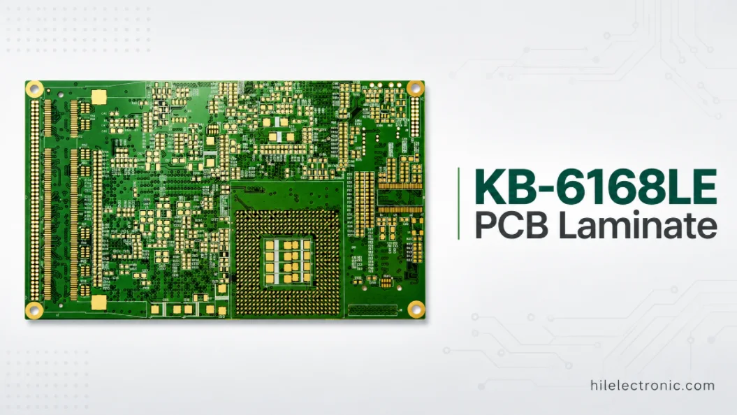
KB-6168LE PCB Laminate for Low Z-CTE Multilayer PCB Manufacturing
KB-6168LE PCB laminate is a Kingboard high-Tg, anti-CAF,...
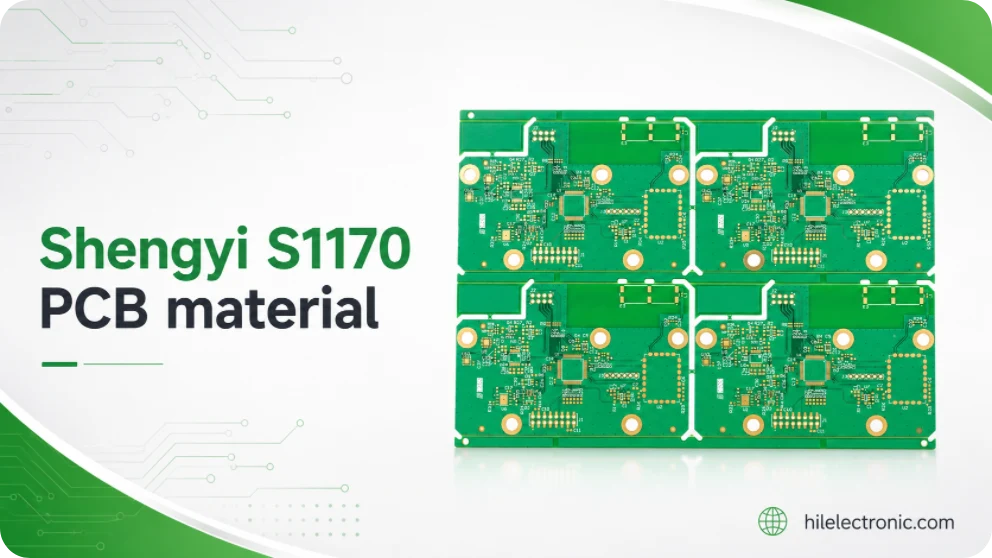
Shengyi S1170 PCB Material for High-Tg Lead-Free Multilayer PCB Manufacturing
Shengyi S1170 PCB material is a lead-free compatible,...

NP-175F PCB Laminate for High-Reliability Multilayer Boards
NP-175F PCB laminate is a Nan Ya high-Tg, filled...

High CTI FR-4 PCB Manufacturing for Insulation-Critical Boards
High CTI FR-4 is used when a PCB design needs stronger...
How to get a quote for PCBs
Let‘s run DFM/DFA analysis for you and get back to you with a report. You can upload your files securely through our website. We require the following information in order to give you a quote:
-
- Gerber, ODB++, or .pcb, spec.
- BOM list if you require assembly
- Quantity
- Turn time
In addition to PCB manufacturing, we offer a comprehensive range of electronic services, including PCB design, PCBA, and turnkey solutions. Whether you need help with prototyping, design verification, component sourcing, or mass production, we provide end-to-end support to ensure your project’s success.
For PCBA services, please provide your BOM (Bill of Materials) and any specific assembly instructions. We also offer DFM/DFA analysis to optimize your designs for manufacturability and assembly, ensuring a smooth production process.