
Rigid Flex PCB Manufacturer and Manufacturing Process

Rigid-flex PCB manufacturing combines rigid PCB fabrication and flexible circuit processing in one integrated board structure. Compared with standard rigid PCB production, the process is more demanding because it must control two very different material systems within the same product. The rigid sections must provide dimensional stability and assembly strength, while the flexible sections must maintain bendability, fatigue resistance, and long-term interconnection reliability.
Because of this, the steps to manufacture rigid-flex PCB involve much more than simply bonding a flex circuit to a rigid board. The complete process includes rigid and flex material preparation, separate circuit formation, coverlay lamination, multilayer bonding, secondary drilling, metallization, outer layer imaging, solder mask, profiling, testing, and final inspection. Every stage must be controlled carefully to ensure that the rigid and flexible portions function together as one reliable finished product.
At Highleap Electronics, our rigid-flex PCB manufacturing workflow is built around process stability, material compatibility, and reliable interconnection between rigid and flexible sections. This is particularly important for products that must meet both compact packaging and long-term mechanical reliability requirements.
Materials Used in Rigid Flex PCB Manufacturing
Rigid-flex PCB construction uses both flexible circuit materials and rigid PCB materials. Material compatibility is a critical part of the process because different materials respond differently to heat, pressure, drilling, and dimensional movement during fabrication.
Flexible Section Materials
- Polyimide PI: The most widely used flex base material because of its excellent heat resistance, flexibility, chemical stability, and dielectric performance.
- Polyester PET: A lower-cost alternative used in less demanding applications, though it offers lower temperature resistance than polyimide.
- Rolled Annealed RA Copper: Commonly preferred for flex areas because it provides better ductility and fatigue resistance during bending.
- Electrodeposited ED Copper: More economical, but generally less suitable for dynamic flexing than RA copper.
- Adhesive Systems: Acrylic and epoxy adhesives are used depending on the flex construction and lamination requirements.
- Adhesiveless Flex Core: Used for thinner constructions, improved flexibility, and better thermal performance.
- Coverlay: Usually polyimide film laminated over the flex circuitry to provide insulation, mechanical protection, and environmental resistance.
- Stiffeners: PI, FR4, stainless steel, or other reinforcement materials are added where local support is needed.
Rigid Section Materials
- FR4 Core: The most common rigid base material for structural support and dimensional stability.
- Prepreg: Used to bond rigid multilayer structures.
- No-Flow Prepreg: Often used in rigid-flex lamination to prevent excessive resin flow into flex areas.
- Copper Foil: Used to form the conductive layers in the rigid portions of the board.
The final rigid-flex stack-up must be designed and manufactured around the interaction of these materials, especially in transition areas where rigid and flex zones meet. In projects where the flexible section design is a major performance factor, the material strategy is closely related to the requirements of flexible PCB construction as well.
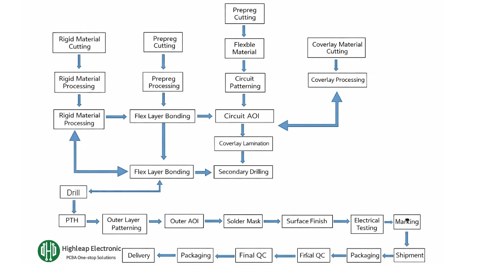
Steps to Manufacture Rigid Flex PCB
- Rigid Material Cutting: Large rigid copper-clad laminate panels are cut into production-size sheets according to the stack-up and panelization plan. This stage ensures that the rigid materials are prepared to match the manufacturing route and tooling requirements.
- Flex Material Cutting: The original roll materials used for the flexible sections, such as polyimide substrate, adhesive, coverlay, and PI reinforcement materials, are cut into the required working size. This preparation is important because flex materials are thinner and more dimensionally sensitive than rigid laminates.
- Primary Drilling: Initial drilling is performed to create tooling holes, alignment holes, and electrical interconnection holes required in the early stages of the build. Hole accuracy at this stage affects later registration and plating reliability.
- Black Hole or Conductive Hole Treatment: A conductive treatment is applied to the hole walls so that metallization can begin. In some process routes, carbon-based conductive treatment is used to prepare the drilled holes for subsequent copper plating.
- Primary Copper Plating: Copper is deposited and plated onto the hole walls and board surface to establish conductivity and prepare the panel for imaging and circuit formation.
- Exposure Alignment: The film artwork is aligned accurately with the drilled panel after dry film lamination. Correct alignment is essential so that the image pattern matches the hole locations and the intended circuit layout.
- Developing: The unexposed dry film is removed, leaving only the imaged resist pattern on the board surface.
- Etching: Unprotected copper is chemically etched away, leaving the circuit traces and pads defined by the patterned resist.
- AOI Inspection: Automated optical inspection is carried out to detect open circuits, short circuits, under-etch, over-etch, and other line defects before the panel proceeds to later processing stages.
- Flex Coverlay Lamination: A protective coverlay film is applied over the flex circuits to prevent oxidation, provide insulation, and preserve the flexibility of the product. This stage is one of the defining differences between flex processing and rigid PCB processing.
- Coverlay Pressing: The coverlay and any reinforcement materials are bonded using controlled heat and pressure so that the coverlay adheres properly without bubbles, wrinkles, or insufficient sealing around the circuit areas.
- Punching: The partially processed flex working panel is cut or punched into the required intermediate size using mechanical punching tools or matching process equipment, depending on the product design.
- Secondary Lay-Up: The prepared flex sections and rigid board sections are stacked together according to the rigid-flex layer structure. Correct lay-up is essential for maintaining alignment and ensuring a stable final laminated structure.
- Secondary Lamination: The stacked rigid and flex materials are laminated together into one integrated panel structure. This stage uses carefully selected prepreg and bonding materials to achieve both structural strength in rigid zones and preserved flexibility in the required areas.
- Secondary Pressing: Under vacuum and controlled thermal pressure, the rigid-flex stack is fused into a single bonded structure. This process must prevent voids, delamination, resin overflow, and misalignment while maintaining the integrity of both rigid and flexible sections.
- Secondary Drilling: Additional holes are drilled into the laminated rigid-flex structure to create the required electrical interconnections between rigid and flex layers in the final board build.
- Plasma Cleaning: Plasma treatment is used to clean the hole walls and surfaces more effectively than conventional wet cleaning methods. This improves metallization reliability and adhesion in later processing.
- Chemical Copper Deposition for the Rigid-Flex Stack: A thin electroless copper layer is deposited in the drilled holes to establish initial conductivity across the newly formed interconnection structure.
- Electrolytic Copper Plating: Electroplating builds up copper thickness in the holes and on the surface to meet electrical and structural reliability requirements. This is a critical step for plated through-hole quality and long-term product reliability.
- Dry Film Lamination for Outer Layer Circuitry: A layer of photosensitive dry film is laminated onto the copper-plated board surface in preparation for outer layer pattern transfer.
- Outer Layer Exposure and Developing: The outer layer circuit image is transferred by exposure, and the unexposed resist is removed so that the desired outer circuitry can be formed accurately.
- Outer Layer Etching: The excess copper outside the required circuit pattern is etched away, leaving the final outer layer traces and pads.
- AOI Verification of Outer Layer Circuitry: Another AOI step is performed after outer layer circuit formation to confirm that no open or short defects remain in the finished pattern.
- Solder Mask Screen Printing on Rigid Areas: Solder mask is applied to the rigid board surfaces to protect the copper circuitry, improve insulation, and support later assembly operations.
- Solder Mask Exposure and Curing: The solder mask is imaged and hardened so that it remains only in the required protective areas and achieves stable adhesion.
- Surface Finish: Surface finish such as ENIG is applied to exposed pads to prevent oxidation and improve solderability during assembly.
- Laser De-paneling or Flex Window Opening: Laser cutting may be used to remove rigid material in designated areas, expose the flex portion, or define complex rigid-flex transition structures with high precision.
- Stiffener or Reinforcement Attachment: Steel pieces, FR4 stiffeners, polyimide stiffeners, or other reinforcement materials are attached in specific areas to increase local support, thickness, or assembly stability.
- Electrical Testing: Flying probe or fixture-based testing is used to check for opens, shorts, and continuity problems to ensure that the board meets the required electrical performance.
- Silkscreen Printing: Symbols, reference marks, logos, and identification information are printed onto the board to assist later assembly, inspection, and traceability.
- CNC Routing or Final Profiling: CNC milling or routing is used to machine the final board outline according to customer dimensions and tolerance requirements.
- Final Quality Control FQC: The finished rigid-flex PCB undergoes complete appearance inspection, dimensional verification, workmanship review, and structural evaluation according to internal quality standards and customer requirements.
- Packaging and Shipment: Approved boards are packaged using antistatic protection, moisture control, and suitable transportation safeguards, then stored or shipped according to customer delivery requirements.
How the Manufacturing Flow Is Typically Divided in Practice
Although the complete process can be listed as a long step-by-step sequence, rigid-flex PCB manufacturing is usually managed in several major production stages:
- Material preparation stage: rigid and flex materials are cut, organized, and prepared for separate processing.
- Flex circuit formation stage: drilling, conductive treatment, imaging, etching, AOI, and coverlay lamination are completed for the flex portion.
- Rigid-flex bonding stage: rigid and flex sections are stacked, laminated, and pressed into one structure.
- Secondary interconnection stage: drilling, plasma cleaning, copper deposition, and copper plating are used to establish reliable electrical interconnection through the laminated structure.
- Outer layer finishing stage: outer circuitry, solder mask, surface finish, profiling, and marking are completed.
- Verification stage: testing, final inspection, and packaging ensure the product is ready for shipment or assembly.
This staged view helps customers understand why rigid-flex PCBs require longer and more tightly controlled manufacturing workflows than ordinary rigid boards. For early-stage programs, this is also why many teams begin with a prototype PCB build before moving into volume production.

Why Rigid Flex PCB Manufacturing Is More Difficult Than Standard PCB Fabrication
Rigid-flex PCB production is more complex because it combines different material systems and different process expectations in one product. The flex section must remain bendable, while the rigid section must provide structural stability, dimensional accuracy, and assembly reliability.
The main manufacturing difficulties include:
- Thin flex material handling: flexible materials are soft and thin, so they are more likely to wrinkle, stretch, or jam during transport and processing.
- Dimensional movement: flex materials generally show lower dimensional stability than FR4, making alignment more difficult.
- Coverlay quality control: poor coverlay lamination can lead to bubbles, voids, poor insulation, or reduced flexibility.
- Lamination control: rigid-flex structures are highly sensitive to resin flow, pressure balance, and heat profile.
- Plated hole reliability: interconnections between rigid and flex sections must maintain conductivity under thermal and mechanical stress.
- Transition area processing: rigid-to-flex transition zones are often the most sensitive mechanical and structural parts of the board.
Because of these factors, successful rigid-flex PCB production requires experience in both multilayer rigid PCB manufacturing and flexible circuit processing. In higher-density layouts, the same registration and interconnection discipline becomes even more important in builds involving HDI PCB structures.
Critical Process Control Points in Rigid Flex PCB Manufacturing
Material Storage and Preparation
Polyimide materials, coverlay, prepreg, and other bonding materials should be stored and handled under controlled conditions. Moisture absorption and dimensional change must be managed before critical processes such as lamination and imaging.
Registration and Exposure Accuracy
Because rigid-flex boards contain both rigid and flexible materials, registration accuracy must be managed carefully throughout drilling, imaging, and lay-up. Any misalignment can affect hole reliability, conductor spacing, and final circuit yield.
Lamination Pressure and Resin Flow
Rigid-flex lamination is one of the most important control points in the process. Pressure, temperature, dwell time, and resin flow behavior must be balanced so that the rigid zones bond correctly without damaging the flex areas.
Hole Wall Quality and Metallization
The reliability of plated through-holes depends on drilling quality, hole wall preparation, plasma cleaning effectiveness, copper deposition, and electroplating thickness. Poor control here can cause intermittent failure or long-term reliability issues.
Flex Area Protection
Throughout processing, the flex sections must be protected from scratches, overstress, contamination, and thermal damage. Improper handling can reduce bend performance or create hidden defects.
Inspection Discipline
Rigid-flex PCB manufacturing requires more than end-of-line inspection. AOI, electrical testing, dimensional checks, visual workmanship inspection, and structural evaluation are all essential parts of process control. In production environments where process verification is critical, additional checks may be supported by comprehensive inspection methods.
Precautions for Manufacturing Rigid Flex PCBs
To maintain consistent quality and reduce production risk, manufacturers should pay attention to the following precautions:
- Select the correct material system for both rigid and flexible areas according to the end application.
- Control bend area design carefully so traces, vias, coverlay openings, and stiffeners do not create stress concentration.
- Use no-flow prepreg where required to prevent excessive resin overflow during lamination.
- Complete flex processing before final rigid-flex bonding when necessary to manage expansion and contraction more effectively.
- Maintain stable environmental conditions such as temperature, humidity, and cleanliness during production.
- Protect flex sections during handling and transportation within the factory.
- Verify both electrical and mechanical reliability through testing and final inspection before shipment.
These precautions are important because rigid-flex PCBs are often used in compact, high-value, and reliability-sensitive products where failure can be difficult and expensive to correct after assembly. If the board will move directly into product build, manufacturability should also be considered together with downstream PCB assembly requirements.
Frequently Asked Questions About Rigid Flex PCB Manufacturing
What is the rigid flex PCB manufacturing process
The rigid flex PCB manufacturing process combines flexible circuit fabrication and rigid PCB production in one integrated structure. It typically includes material preparation, drilling, conductive hole treatment, copper plating, circuit imaging, etching, coverlay lamination, rigid-flex bonding, secondary drilling, outer layer processing, testing, and final inspection.
Why is rigid flex PCB harder to manufacture than standard PCB
Rigid flex PCB is more difficult to manufacture because it combines rigid and flexible materials with different thermal and mechanical behaviors. The process must maintain dimensional stability in the rigid sections while preserving bendability and fatigue resistance in the flex areas. Lamination, alignment, and plated hole reliability are all more demanding than in standard rigid PCB fabrication.
What materials are used in rigid flex PCB fabrication
Rigid flex PCBs typically use FR4 cores and prepreg in the rigid sections, while the flexible sections usually use polyimide film, rolled annealed copper, coverlay, adhesive systems, and optional stiffeners. No-flow prepreg is often used during rigid-flex lamination to control resin flow and protect the flex areas.
What is the most critical step in rigid flex PCB manufacturing
Several steps are critical, but lamination and interconnection reliability are usually the most important. Secondary lay-up, lamination, drilling, plasma cleaning, copper deposition, and copper plating determine whether the rigid and flex sections will remain mechanically stable and electrically reliable in the finished board.
How are holes made reliable in rigid flex PCB
Reliable plated holes depend on accurate drilling, proper conductive hole treatment or chemical copper deposition, effective plasma cleaning, and controlled electroplating thickness. These steps ensure strong copper coverage on the hole walls and stable electrical connection between rigid and flexible layers.
Does rigid flex PCB use solder mask or coverlay
Rigid flex PCBs usually use both, but in different areas. The rigid sections typically receive solder mask, while the flex sections are usually protected by polyimide coverlay. This combination provides insulation, circuit protection, and the flexibility required in the bend areas.
How is rigid flex PCB tested before shipment
Rigid flex PCBs are typically tested through electrical continuity and isolation testing, AOI inspection, dimensional verification, appearance inspection, and final quality control review. Depending on the application, additional reliability checks may also be required.
What should buyers check when choosing a rigid flex PCB manufacturer
Buyers should review whether the manufacturer has proven experience in both rigid PCB fabrication and flexible circuit processing, whether the factory can control lamination and plated hole reliability, and whether it can support prototype, low-volume, and production builds with stable quality control and inspection procedures. For project-specific requirements, they can also discuss the build directly with the manufacturer through the contact page.
Conclusion
The steps to manufacture rigid-flex PCB involve a complete sequence of rigid material preparation, flex material preparation, drilling, conductive hole treatment, copper plating, circuit imaging, etching, AOI, coverlay lamination, rigid-flex lay-up, secondary lamination, plasma cleaning, metallization, solder mask, surface finishing, profiling, testing, and final inspection. This is a more demanding process than standard PCB fabrication because the board must combine the structural performance of rigid PCBs with the bendability of flexible circuits in one stable product.
For engineers and buyers, understanding the full rigid-flex manufacturing route helps improve design choices, clarify sourcing requirements, and reduce project risk. For manufacturers, consistent quality depends on disciplined control of materials, lamination, hole metallization, dimensional stability, and inspection at every major stage of production. With the right process management, rigid-flex PCBs can deliver the space savings, integration, and reliability required by advanced electronic systems.
Sabrina has over 18 years of experience in the PCB industry, with a strong background in CAM engineering and PCB file review. She supports PCB projects from prototype to volume production, focusing on manufacturability and process reliability. Her work helps engineering teams reduce production risk and achieve stable, high-quality PCB manufacturing results.

Related Articles
Rogers RT/duroid 6010.2LM PCB Manufacturer and Fabrication Service
Highleap Electronics reviews and manufactures Rogers RT/duroid 6010.2LM high-Dk microwave PCBs, including controlled impedance, multilayer and hybrid fabrication, assembly, testing, cost factors, and RFQ requirements.

Panasonic R-5785(N) MEGTRON 7 PCB Manufacturer and Fabrication
Highleap Electronics manufactures Panasonic R-5785(N) MEGTRON 7 ultra-low-loss high-layer-count PCBs for AI servers, switches and backplanes, with H-VLP copper review, stackup, back drilling, PCBA, testing, cost and RFQ guidance.
Panasonic MEGTRON 6N PCB Manufacturer for Servers and AI Hardware
Highleap Electronics manufactures Panasonic MEGTRON 6N R-5775(N) high-speed multilayer PCBs for servers, AI hardware, switches and backplanes, with stackup, back drilling, assembly, testing, cost and RFQ guidance.