
HDI PCB CAM Workflow | Define SMD, Vias, and Drill Rules

HDI PCB CAM production is one of the most technically demanding areas in PCB manufacturing. With increasing IC integration and high-density assembly requirements, HDI mobile boards often feature complex outlines, dense routing, and tight via arrangements.
These challenges make CAM processing time-consuming and error-prone—especially under pressure for high quality and fast delivery. Based on real-world production experience, this article shares practical insights into handling SMDs, blind vias, solder mask, and shape processing in HDI PCB CAM workflows.
Defining SMD Pads in HDI PCB CAM Workflows
In HDI PCB CAM processing, accurate SMD (Surface Mount Device) definition is the first critical step. During PCB manufacturing, processes such as graphic transfer and etching can alter the final copper features. To ensure compliance with customer acceptance standards, CAM engineers must apply compensation adjustments to both traces and SMDs independently. Failure to define SMD pads correctly can result in undersized or missing pads, which directly affects solderability and assembly reliability.
Handling CSP Pads and Blind Vias in HDI Mobile Boards
Many HDI mobile board designs involve 0.5mm Chip Scale Packages (CSPs) with pad diameters as small as 0.3mm. In some cases, these CSP pads overlap with blind via pads, both measuring exactly 0.3mm, which may lead to misalignment or pad merging if not handled properly in CAM.
Using Genesis2000, you can prevent these issues with the following steps:
Step-by-Step SMD Definition in Genesis2000
- Close all drill layers related to blind and buried vias.
- Define SMDs based on customer design requirements.
- Use the FeaturesFilterpopup and Referenceselectionpopup functions to locate CSP-related pads from both top and bottom layers, and move them to temporary layers (t layer for top, b layer for bottom).
- In the t layer, remove all 0.3mm pads that overlap with blind vias and delete redundant CSP pads from the original top layer.
- Rebuild the CSP pads manually according to the specified pad size, location, and count, then define them as SMDs. Copy the corrected pads back to the TOP layer and add corresponding via pads if needed.
- Repeat the same process for the b layer.
- Finally, scan the Gerber files to detect any SMDs that are missing or duplicated.
Benefits of This Optimized CAM Process
Compared to traditional CAM practices, this targeted HDI PCB CAM method offers:
- A clear workflow for defining SMDs in dense HDI designs
- Fewer processing steps, reducing time and manual error
- Better compatibility with blind via + CSP pad overlap scenarios
- Improved accuracy and first-pass yield
Removing Non-Functional Pads in HDI PCB CAM
Another important operation in HDI PCB CAM workflows is the removal of non-functional pads (NFPs)—pads that are not connected to any net on certain layers. These pads can impact signal integrity, increase layer complexity, and pose manufacturing challenges, especially in high-density HDI mobile board designs.
Using a typical 8-layer HDI PCB as an example, the CAM process involves two main NFP removal steps:
Step-by-Step NFP Removal in CAM
- Remove non-metalized hole pads on the top and bottom layers using the NFPRemovel function.
- Remove via-related NFPs:
- Close all drill layers except vias
- Set Removeundrilledpads in NFPRemovel to NO
- Remove non-functional pads from layers 2 to 7
- Remove buried via NFPs:
- Close all drill layers except buried vias
- Again, set Removeundrilledpads to NO
- Remove non-functional pads from layers 3 to 6
This process ensures clean internal layers and helps reduce unnecessary copper features, which can improve etching uniformity and minimize manufacturing risks.
Why This NFP Removal Method Works for HDI CAM
This method is especially suitable for CAM engineers handling multilayer HDI PCB designs because:
- It uses a clear layer-based workflow, easy to learn and execute
- Compatible with Genesis2000 CAM software
- Reduces internal copper clutter, which is essential for fine-line etching and laser via alignment
For CAM operators—especially those new to HDI stack-up processing—this step-by-step method offers a simple and effective approach to non-functional pad removal.

Laser Drilling in HDI PCB CAM Processing
Laser drilling is a vital step in HDI PCB CAM, especially for creating high-density blind vias typically around 0.1mm in diameter. In our production process, we use CO₂ laser technology, which is effective for drilling through organic materials such as RCC or PI, but not copper foil due to copper’s high melting point and low infrared absorption.
Using Conformal Mask for CO₂ Laser Processing
Since CO₂ lasers cannot burn through copper, a conformal mask process is applied in CAM. This involves etching the copper foil at the laser-drilled via locations so that the laser can access the dielectric layer directly. To support this process, CAM engineers must generate an exposure hole film based on the via positions during data preparation.
CAM Drill Checks to Ensure Design Rules
To maintain structural integrity and ensure that copper foil remains at the bottom of the outer layers, the minimum spacing between blind vias and buried vias must be at least 4 mils. In Genesis2000, CAM engineers can perform this validation using the following path:
Analysis → Fabrication → Board-Drill-Checks
This helps detect and flag violations in via spacing, which could otherwise lead to drilling defects or improper via formation during manufacturing.
Incorporating laser drilling into HDI PCB CAM workflows requires both material knowledge and software validation. Using CO₂ laser in combination with conformal masking and careful CAM rule checks ensures via precision and process reliability in high-density HDI mobile boards.
Plugging Holes and Solder Mask Handling in HDI PCB CAM
In the HDI PCB CAM workflow, the outer layers typically use RCC (Resin Coated Copper) materials, which have thin dielectric layers and low resin content. According to experimental data, when the finished board thickness exceeds 0.8mm, and the metallized slot dimensions are ≥ 0.8mm × 2.0mm or the metallized hole diameter is ≥ 1.2mm, two sets of plug hole files must be prepared. This means the holes require double plugging:
- The inner layers use resin scraping and plugging.
- The outer layers are plugged directly with solder mask ink before solder mask application.
Challenges of Vias Near SMD Pads During Solder Mask Process
In the solder mask production process, vias located on or near SMD pads pose a risk of ink leakage during solder mask exposure. Since customers typically require all vias to be plugged, CAM engineers must carefully manage via placement and solder mask openings to avoid solder mask defects.
CAM Solutions for Via and Solder Mask Interaction
The common CAM approach is:
- Move vias away from SMD pads if possible to prevent overlap.
- If vias cannot be relocated, apply one of the following solder mask adjustments:
- For vias covered by solder mask, add transparent dots on the solder mask layer, sized 3 mils smaller than the finished hole on one side.
- For vias touching the solder mask opening, add transparent dots that are 3 mils larger than the finished hole on one side. (This is used when customers allow minor solder mask ink coverage on the pad.)
Proper handling of plugging holes and solder mask layers in the HDI PCB CAM process is essential to ensure manufacturing quality and solder joint reliability, especially for high-density designs with tight SMD and via placement.

Shape Processing in HDI PCB CAM Panel Design
In HDI PCB CAM production, boards are often delivered in panelized formats with complex and non-standardized outlines. Customers usually provide a CAD drawing (typically in .DWG format) that includes the panel outline, stamp holes, positioning holes, and optical alignment points.
Efficient Shape Import via DXF in Genesis2000
Rather than manually redrawing the panel outline in Genesis2000, which is time-consuming and error-prone, CAM engineers can simplify the process by converting the customer’s CAD file:
- Open the .DWG file.
- Use the “Save As” function and change the file type to: AutoCAD R14/LT98/LT97 DXF (*.DXF)
- In Genesis2000, import the .DXF file just like a Gerber file.
This method allows CAM engineers to accurately and efficiently bring in:
Benefits for HDI Panel Production
This DXF import approach not only improves speed but also reduces the risk of dimensional errors—especially valuable in high-precision HDI PCB panels. It ensures accurate alignment for subsequent drilling, routing, and assembly processes.
Milling the Outline Border in HDI PCB CAM
In HDI PCB CAM processing, milling the outline border is a critical step. Unless a customer specifically requests exposed copper, standard fabrication practices require copper foil to be pulled back slightly from the board edge. This prevents copper delamination or flipping during milling.
Risk of Open Circuits Due to Narrow Copper Ends
However, pulling back the copper may create ultra-narrow traces near the edge. For example, if two copper ends (A) are close to the border and:
- Do not belong to the same electrical net
- Are less than 3 mils wide
Then the resulting shape may be unmanufacturable and could lead to an open circuit. These types of issues are not visible in the standard Genesis2000 analysis reports.
CAM Solution: Secondary Net Comparison with Modified Edge Pullback
To detect and resolve this issue, a secondary net comparison is required:
- Manually remove an additional 3 mils of copper inward from the board edge.
- Re-run the network comparison in Genesis2000.
- Interpret the result:
- If no open circuit is found: the two copper ends either belong to the same net, or the width after trimming is ≥ 3 mils, which is manufacturable.
- If an open circuit occurs: the copper width is too narrow or the nets are isolated—widen the copper foil to ensure connectivity and reliable production.
This method provides a practical approach to preventing undetected CAM issues during outline milling in HDI PCBs, enhancing yield and ensuring compliance with production standards.
Conclusion
The demand for high-integration ICs and high-density interconnection assembly technology has propelled HDI boards to the forefront of the PCB manufacturing industry. However, their complex designs and dense wiring present significant challenges during CAM production, often resulting in delays and inaccuracies. To ensure top-notch quality and timely delivery, CAM engineers have developed valuable insights through continuous practice and refinement.
Key areas of focus include accurate SMD definition, streamlined non-functional pad removal, precision laser drilling techniques, efficient handling of plug holes and solder masks, optimized shape production, and meticulous border milling. By systematically addressing these challenges and utilizing advanced CAM strategies, professionals can achieve greater efficiency and precision in HDI board production. The result is the delivery of superior-quality PCBs that meet the evolving demands of the market.

Recommended Posts
PCB Trace Width Calculator: How to Size Traces for Current, Voltage Drop, and Impedance
Figure 1. A PCB trace width calculator is a starting point...
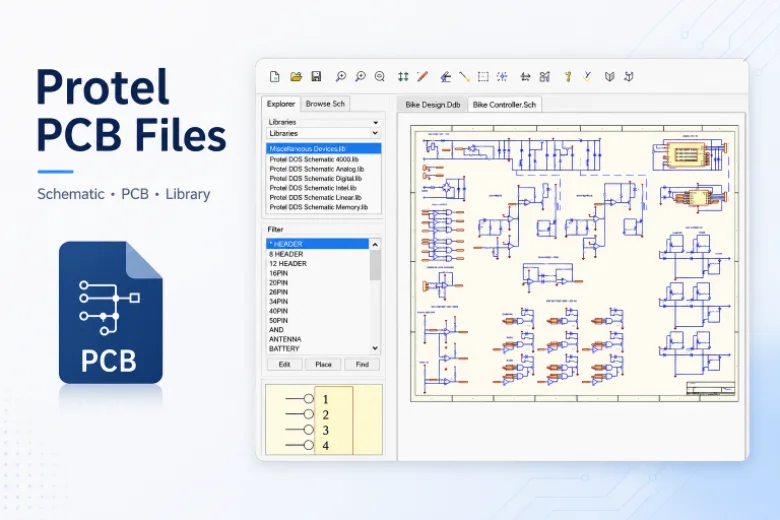
Protel PCB: Is It the Same as Altium Designer, and How to Open Legacy Protel Files
Figure 1. Legacy Protel PCB files often need review before...
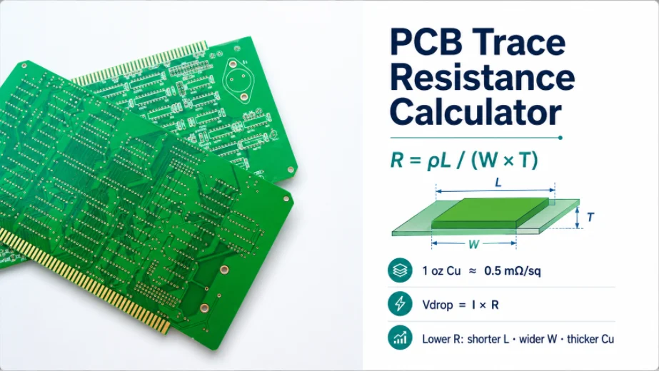
PCB Trace Resistance Calculator: How to Calculate Trace Resistance and Voltage Drop
Figure 1. PCB trace resistance affects voltage drop, heat...
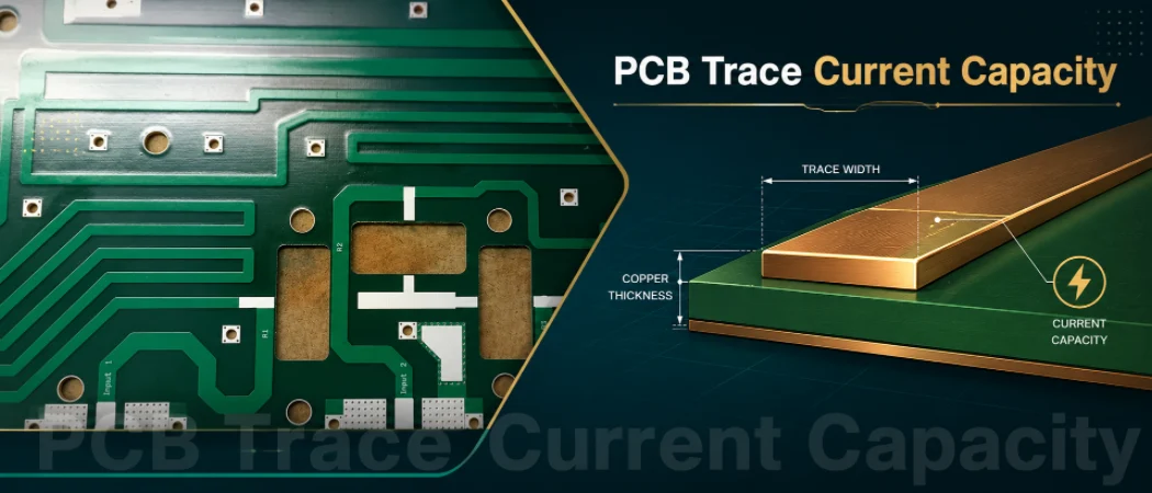
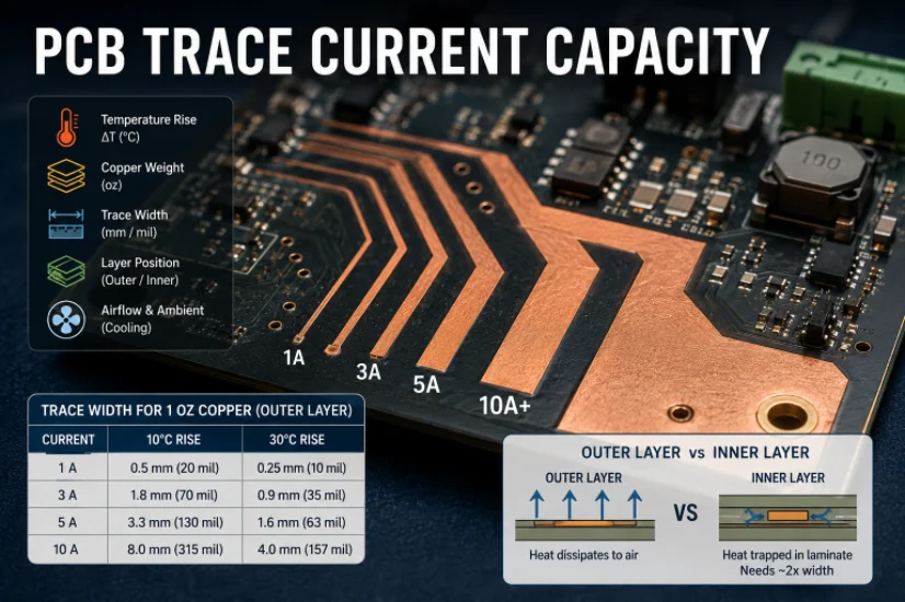
PCB Trace Current Capacity: Width, Copper Weight, and IPC-2221
Figure 1. PCB trace current capacity depends on copper...
How to get a quote for PCBs
Let us run DFM/DFA analysis for you and get back to you with a report.
You can upload your files securely through our website.
We require the following information in order to give you a quote:
-
- Gerber, ODB++, or .pcb, spec.
- BOM list if you require assembly
- Quantity
- Turn time
In addition to PCB manufacturing, we offer a comprehensive range of electronic services, including PCB design, PCBA (Printed Circuit Board Assembly), and turnkey solutions. Whether you need help with prototyping, design verification, component sourcing, or mass production, we provide end-to-end support to ensure your project’s success. For PCBA services, please provide your BOM (Bill of Materials) and any specific assembly instructions. We also offer DFM/DFA analysis to optimize your designs for manufacturability and assembly, ensuring a smooth production process.