
Why PCB Testing Is Necessary: The Ultimate Guide to PCBA Inspection Methods

Table of Contents
Executive Summary: PCB testing is a critical risk mitigation strategy that goes far beyond simple visual checks. A comprehensive testing protocol encompasses structural validation (AOI, X-Ray), electrical verification (ICT, Flying Probe, Impedance), and reliability assurance (Stress and Burn-in testing). This guide breaks down every essential PCB testing method to help you choose the right inspection strategy and prevent costly field failures.
1. The True Cost of Skipping PCB Testing
For hardware engineers and product managers, discovering a fatal flaw in a printed circuit board after it has hit the market is the ultimate nightmare. Why is PCB testing necessary? Because the cost of fixing a defect increases exponentially at each stage of production.
- Design Stage: 1x Cost to fix (Updating Gerber files)
- Prototyping Stage: 10x Cost to fix (Reworking a few boards)
- Mass Production: 100x Cost to fix (Scrapping a whole batch)
- In the Field: 1000x+ Cost to fix (Product recalls, brand damage, and warranty claims)
At Highleap Electronic, we implement rigorous testing protocols throughout the PCB fabrication and assembly phases to ensure that your products function flawlessly in their intended environments.
2. The PCB Testing Method Matrix
There is no one-size-fits-all approach to PCBA testing. The optimal testing suite depends on component density, high-speed requirements, and operating environments. Here is a comprehensive breakdown of industry-standard testing methods.
| Testing Category | Specific Method | What It Detects / Verifies | Best Suited For |
|---|---|---|---|
| Visual & Structural | AOI (Automated Optical) | Missing components, polarity, tombstoning, surface bridges. | Every batch, standard SMT lines. |
| AXI (2D/3D X-Ray) | Hidden solder voids, BGA/QFN joint integrity, internal shorts. | High-density boards with bottom-terminated components. | |
| Electrical Performance | Flying Probe / ICT | Opens, shorts, resistance, capacitance across all nodes. | Prototypes (FPT) and High-Volume Mass Production (ICT). |
| TDR (Impedance Test) | Signal integrity, trace impedance matching. | High-speed digital and RF communication boards. | |
| Functional Test (FCT) | Real-world performance, firmware execution, voltage levels. | Final stage verification for fully assembled products. | |
| Reliability & Stress | Burn-in & Aging Test | Early component failure (infant mortality) under continuous load. | Mission-critical applications (Medical, Automotive). |
| Environmental Stress | Thermal shock, vibration, humidity resistance, peel strength. | Aerospace, industrial control, and ruggedized electronics. |
3. Visual & Structural Inspection
Automated Optical Inspection (AOI)
AOI uses high-resolution cameras to compare the assembled board against the original Gerber/CAD data. It is highly effective at catching surface-level defects like tombstoning, missing parts, and incorrect component orientation. However, AOI cannot see beneath components.
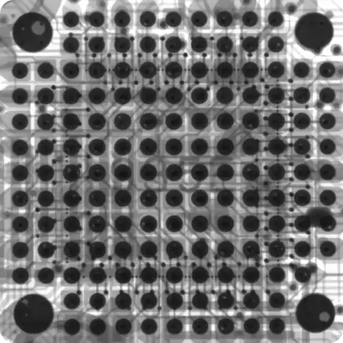
Automated X-Ray Inspection (AXI)
As designs become denser, components like Ball Grid Arrays (BGAs) and QFNs hide their solder joints beneath the package. 2D and 3D X-Ray Inspection penetrates the IC packages to inspect the solder joints underneath. It is the only reliable way to detect hidden solder voids, insufficient wetting, and internal shorts, ensuring voiding remains below the acceptable IPC standard threshold (typically < 25%).
4. Electrical & Signal Integrity Testing
Flying Probe Test vs. In-Circuit Testing (ICT)
To verify the electrical connections (checking for fatal opens and shorts):
- Flying Probe Test (FPT): Uses movable robotic probes to test the board. Ideal for a PCB prototype because it requires no custom fixtures.
- In-Circuit Testing (ICT): Uses a custom “bed of nails” fixture to test the entire board simultaneously. Extremely fast and cost-effective for large-scale mass production.
Impedance Testing (TDR)
For modern high-speed designs (like DDR memory buses, PCIe, or RF circuits), simply checking for continuity is not enough. Time Domain Reflectometry (TDR) is used to measure trace impedance. If the impedance fluctuates due to improper trace width or dielectric thickness, signal reflection will occur, corrupting high-speed data. TDR ensures your board meets strict signal integrity tolerances.
5. Reliability & Environmental Stress Testing
Will your PCBA survive in the real world? For products deployed in harsh environments, physical and thermal testing is mandatory:
- Burn-in and Aging Testing: The board is powered on and run at maximum capacity in a controlled oven (often at 85°C to 125°C) for 24 to 168 hours. This forces weak components to fail before the product leaves the factory (eliminating “infant mortality”).
- Thermal Shock & Cycling: The PCB is rapidly moved between extreme cold and extreme heat. This tests the coefficient of thermal expansion (CTE) mismatch, ensuring that vias and solder joints won’t crack under temperature stress.
- Mechanical Stress & Vibration: Simulates drops, shipping conditions, and engine vibrations to ensure heavy components (like inductors or large capacitors) do not shear off the board.
- Peel Strength & Lamination Test: Tests the physical adhesion of the copper foil to the dielectric substrate, ensuring the PCB layers won’t delaminate under high heat.
6. Optimize Your Board: Design for Testability (DFT)
Testing is only as good as the board’s design. To reduce testing costs and time, engineers should adopt Design for Testability (DFT) principles during the layout phase:
- Include adequate test points (pads) for all critical nodes, preferably on one side of the board.
- Design HDI boards with proper impedance control guidelines in mind to guarantee passing TDR tests.
- Leave clearance around tall components so X-Ray angles and ICT probes are not obstructed.
7. Ensure Zero Defects with Highleap Electronic
At Highleap Electronic, we don’t just assemble boards; we guarantee their performance in the real world. Whether you need an aging test for a rugged industrial controller, strict TDR impedance control for high-speed routing, or precision 3D X-Ray for a dense BGA layout, our facility is equipped with state-of-the-art testing equipment.
Don’t leave your product’s reliability to chance. Incorporating the right testing methods from the start ensures a smooth transition from prototype to flawless mass production.

Related Articles
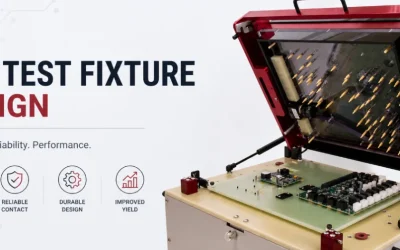
PCB Test Fixture Design: Bed-of-Nails, Flying Probe, and DFT
Compare PCB test fixture options, learn when bed-of-nails beats flying probe, and design test access for faster, repeatable production checks.
RO4003C vs RO4350B: Rogers Datasheet Values, LoPro Foil, and Stackup Choices
Compare RO4003C vs RO4350B using Rogers datasheet values, LoPro foil, Dk, Df, stackup, impedance, and RF PCB fabrication needs.
IPC-A-610 Standard for PCB Assembly Acceptance
Learn what IPC-A-610 covers for electronic assemblies, how Classes 1, 2, and 3 differ, and how buyers should specify assembly acceptance.