
Flex PCB Gold Fingers: Design and Manufacturing

Flex PCB gold fingers are plated edge contacts that create a repeatable electrical interface between a flexible circuit and its mating connector. Their reliability depends on the contact geometry, surface finish, stiffener design, bevel, and the manufacturing controls used to protect the contact area.
This guide explains the design and production decisions that help buyers and engineers specify durable flex PCB gold fingers for repeated insertion, compact packaging, and stable signal transfer.
Table of contents
- What Are Flex PCB Gold Fingers?
- Key Design Requirements
- Surface Finish and Plating
- Manufacturing Controls for Gold Fingers
- Inspection and Reliability Checks
- Working With Highleap Electronics
What Are Flex PCB Gold Fingers?
Gold fingers are exposed conductive pads arranged along a circuit edge. On flex circuits, they commonly connect to ZIF, card-edge, or custom mating connectors. The gold surface resists oxidation and provides a stable contact interface when the copper pattern, pad spacing, and connector specification are aligned.
The term describes the contact area, not a generic decorative finish. The required plating type and thickness should be selected from the connector duty cycle, contact force, environment, and applicable customer specification.
Key Design Requirements
Start with the connector drawing: pad pitch, contact width, insertion direction, keep-out zones, and board-edge tolerance determine the contact pattern. A stiffener is often needed behind the contact area to achieve the thickness and rigidity required by the connector.
- Keep solder mask, coverlay, and exposed copper boundaries clear of the contact path.
- Define pad spacing and finger length from the mating connector rather than a generic rule.
- Specify chamfer or bevel requirements where the connector design calls for guided insertion.

Surface Finish and Plating
For contacts that experience repeated mating, hard gold over a suitable nickel barrier is often selected because it is designed for wear resistance. ENIG may be appropriate for solderable pads, but it should not be assumed to replace a wear-rated contact finish.
Provide the required gold type, thickness range, and plated area in the fabrication notes. This allows the manufacturer to choose a controlled process and avoids applying an unsuitable finish to the full flex circuit.
Manufacturing Controls for Gold Fingers
Reliable gold fingers require clean imaging, controlled plating, accurate edge profiling, and protection from handling damage. The contact area should remain free of fingerprints, scratches, residue, and coverlay encroachment.
Before production, a DFM review should confirm the relationship between copper features, flex outline, stiffener, and connector constraints. This reduces late changes caused by edge tolerance or thickness stack-up conflicts.

Inspection and Reliability Checks
Inspection typically verifies finger width, pitch, edge profile, plating coverage, cosmetic condition, and the absence of shorts or contamination. Electrical testing confirms the finished flex circuit has the intended continuity and isolation before it enters assembly.
For demanding products, the acceptance criteria should define cosmetic limits and any required adhesion, insertion-cycle, or environmental validation with the final connector system.
Working With Highleap Electronics
Highleap Electronics can review flex PCB data, connector requirements, and stack-up details before fabrication. A clear drawing package with the contact finish, stiffener, and inspection requirements helps align the finished circuit with the intended mating interface.
For a manufacturability review, request a PCB quote with the Gerber files, drawing, stack-up, and connector information.
Get a Free PCB & PCBA Quote

Recommended Posts

Flex PCBA Services: Lightweight, Durable, and Ready for Any Application
Unlike traditional rigid PCBs, flexible PCBs use bendable...
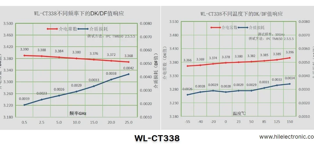
Custom WL-CT338 PCBs: Unlocking Performance for High-Tech Industries
At Highleap Electronic, we specialize in providing custom...

Custom Flex Board Production: Ultra-Long, Extra-Large, and Multi-Layer Designs
Flex boards, also known as flexible circuit boards (FPCs),...

Multilayer Flex PCB Manufacturing One-Stop Service
In today’s world of compact, high-performance, and...
How to get a quote for PCBs
Let us run DFM/DFA analysis for you and get back to you with a report.
You can upload your files securely through our website.
We require the following information in order to give you a quote:
-
- Gerber, ODB++, or .pcb, spec.
- BOM list if you require assembly
- Quantity
- Turn time
In addition to PCB manufacturing, we offer a comprehensive range of electronic services, including PCB design, PCBA (Printed Circuit Board Assembly), and turnkey solutions. Whether you need help with prototyping, design verification, component sourcing, or mass production, we provide end-to-end support to ensure your project’s success. For PCBA services, please provide your BOM (Bill of Materials) and any specific assembly instructions. We also offer DFM/DFA analysis to optimize your designs for manufacturability and assembly, ensuring a smooth production process.