
Heavy Copper PCB for Power Supply Current and Heat

Introduction
Heavy copper PCB technology, defined by copper thickness of 3 oz (105 μm) or greater, has become essential for modern industrial power electronics. These specialized circuit boards address the fundamental challenges of high-current applications where standard PCBs fail to deliver adequate performance.
In industrial power supplies and inverter systems, heavy copper PCB for power supply applications enables reliable operation under extreme electrical and thermal stress while maintaining structural integrity. This article examines the critical design parameters and manufacturing considerations for demanding industrial environments.
The Demands of Industrial Power and Inverter Systems
High Current and Power Density Requirements
Industrial power supplies, motor drives, and welding equipment operate at current levels that generate significant I²R losses and heat concentration. Power electronics PCB designs must accommodate current densities that would cause standard boards to overheat or fail. Inverter PCB design for variable frequency drives routinely handles hundreds of amperes through compact layouts, creating thermal management challenges that require specialized heavy copper PCB solutions.
Environmental and Operational Stress
Industrial environments subject circuit boards to prolonged thermal cycling, mechanical vibration, and chemical exposure. Power modules in manufacturing facilities operate continuously at elevated temperatures while maintaining electrical isolation between high-voltage sections. Traditional PCB constructions lack the thermal conductivity and mechanical robustness needed for industrial environment reliability, leading to premature failure in mission-critical power supply systems.
Why Heavy Copper PCB for Power Supply Applications
High Current Carrying Capacity
Heavy copper PCB constructions allow wider conductor paths without increasing board size, directly reducing resistive losses and voltage drops. The increased copper mass distributes current more evenly across the high current PCB surface, preventing localized heating that degrades solder joints and component reliability:
This page is limited to high-current power supply boards that need heavy copper. For the general board category, start with the power supply circuit board overview; for plating, etching, and manufacturability limits, use the related heavy copper PCB manufacturing.
- Reduced I²R losses – Thicker copper minimizes resistive heating in primary current paths.
- Lower voltage drops – Enhanced conductivity maintains stable operating voltages under load.
- Even current distribution – Wider traces prevent hot spots and thermal stress concentrations.
Superior Thermal Management
The enhanced thermal conductivity of thick copper layers creates effective heat spreading paths from power semiconductors to board edges or mounting surfaces. Heavy copper PCB for power supply modules acts as an integrated heat sink, reducing junction temperatures in IGBTs, MOSFETs, and power diodes. This thermal performance improvement extends component lifespan and enables higher power density designs in inverter applications.
Enhanced Mechanical Strength
The additional copper mass reinforces board structures against warping during reflow and thermal cycling. Plated-through holes with heavy copper barrels demonstrate superior resistance to thermal stress fractures compared to standard constructions. PCB reliability in high-vibration industrial installations depends on this mechanical reinforcement, particularly in large boards carrying heavy power components.

Heavy Copper PCB
Design Considerations for Heavy Copper PCB Power Supply
Copper Thickness Selection
Selecting appropriate copper weight requires analysis of sustained current levels and thermal constraints. PCB design for power modules typically employs 3 oz copper for medium-power applications up to 50A, while high-power inverters may specify 6-10 oz for primary current paths. The copper thickness directly affects manufacturing complexity and cost, requiring balanced optimization against electrical requirements in power supply designs.
Trace Width and Current Density
IPC-2152 standards provide temperature rise calculations based on conductor geometry and copper weight. For heavy copper PCB applications, designers must account for current density limits while maintaining adequate spacing. Thermal vias beneath power components create vertical heat paths to inner copper planes, significantly improving heat dissipation in multilayer power supply constructions.
Insulation and Safety Compliance
Industrial power supplies must meet stringent electrical isolation requirements defined by UL and IEC standards:
- Creepage distance – Increased spacing prevents surface tracking between high-voltage traces.
- Clearance requirements – Air gaps maintain dielectric strength in contaminated environments.
- Material selection – High CTI ratings ensure long-term insulation performance.
Heavy copper boards require careful spacing planning due to higher voltage gradients at trace edges, maintaining safety certification compliance throughout the product lifecycle.
Manufacturing Heavy Copper PCB for Power Supply
Electroplating and Etching Processes
Heavy copper PCB fabrication demands precise control of thick copper plating uniformity across panel surfaces. Advanced electroplating techniques ensure consistent copper distribution in through-holes and on outer layers, preventing weak points in current paths. Etching thick copper requires specialized chemistry and extended process times to achieve clean edge definition without undercutting in power supply board manufacturing.
Lamination Control and Material Selection
High Tg FR-4 materials or polyimide substrates prevent delamination during lead-free soldering and high-temperature operation. Lamination control becomes critical with thick copper layers, as resin flow must fully encapsulate conductor profiles without creating voids. Metal-core PCBs with aluminum or copper bases provide additional thermal management for extremely high-power supply applications.
Surface Finish for Power Applications
ENIG (Electroless Nickel Immersion Gold) offers excellent solderability and contact resistance for high-current connections, while immersion silver provides cost-effective reliability. The surface finish must withstand multiple thermal cycles without degradation, maintaining low contact resistance at power connection points throughout the heavy copper PCB service life in industrial power supply systems.

Switch Mode Power Supply PCBA
Application Examples in Industrial Power Systems
Industrial Power Supply Modules
Switch-mode power supplies for industrial automation employ heavy copper PCB technology to handle rectifier currents and minimize losses in primary-side circuits. The thermal management advantages enable compact power supply designs that meet modern efficiency standards while operating reliably in factory environments with extended temperature ranges.
Motor Drive and Inverter Control
Variable frequency drives and servo amplifiers rely on heavy copper constructions for their power stages, where IGBTs switch hundreds of amperes at kilohertz frequencies:
- Power stage optimization – Heavy copper handles peak currents without excessive heating.
- Gate drive integration – Controlled impedance paths ensure reliable switching performance.
- EMI management – Solid copper planes provide effective shielding and return paths.
Renewable Energy Systems
Solar inverters and energy storage systems process kilowatts of power through circuit boards exposed to wide temperature ranges. Heavy copper PCB for power supply sections in these applications ensures long-term reliability in outdoor installations where service access is limited and failure costs are high in grid-tied and off-grid configurations.
Reliability and Testing for Heavy Copper PCB
Manufacturing Quality Control
Automated optical inspection and X-ray imaging verify inner layer registration and copper plating uniformity before lamination. Cross-sectional analysis confirms plating thickness consistency in through-holes, identifying potential weak points before boards enter production. These quality control measures in heavy copper PCB manufacturing prevent field failures and ensure specification compliance for power supply applications.
Environmental Stress Testing
Thermal cycling between operating extremes validates solder joint integrity and copper adhesion under realistic stress conditions. Vibration testing confirms mechanical robustness in applications subject to motor vibration or transportation shock. Reliability testing protocols specific to power electronics verify that heavy copper PCB constructions meet the extended lifetimes required for industrial power supply equipment.
Conclusion
Heavy copper PCB technology has proven essential for industrial power supply and inverter applications, delivering three critical advantages that standard PCBs cannot match. The enhanced current capacity eliminates thermal failures in high-power circuits, while superior heat spreading extends component lifetimes under continuous operation. Mechanical reinforcement from thick copper layers ensures reliability in demanding industrial environments where vibration and thermal cycling would compromise conventional board constructions.
Highleap Electronics specializes in heavy copper PCB manufacturing for power supply applications:
- Copper weights from 3 oz to 20 oz – Optimized for your specific current requirements.
- Advanced thermal management – Metal-core and thick copper designs for maximum heat dissipation.
- Design support services – DFM analysis ensures manufacturability and performance.
- Full quality traceability – AOI, X-ray inspection, and cross-sectional analysis on every production lot.
Contact our engineering team to discuss your heavy copper PCB power supply requirements and receive expert guidance on design optimization for industrial applications.

Recommended Posts
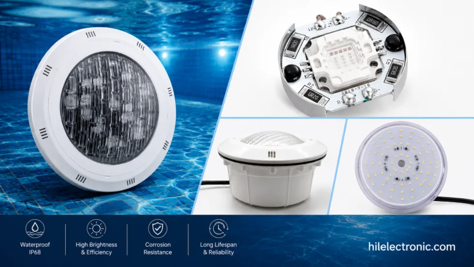
Underwater & Pool LED Light PCBs: IP68 Potted Boards, Low-Voltage Drivers & Safety
Figure 1. LED pool light PCB manufacturing reference....
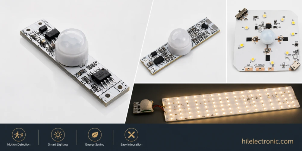
Motion Sensor & Smart LED Light PCBs: Sensor, Control, Driver & Wireless Boards
Figure 1. motion sensor LED light PCB manufacturing...
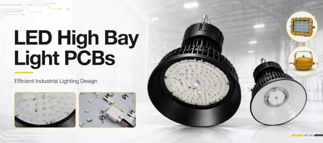
LED High Bay Light PCBs: Metal-Core Light Engines, Drivers & Turnkey Boards Built to Spec
Figure 1. LED high bay light PCB manufacturing reference....
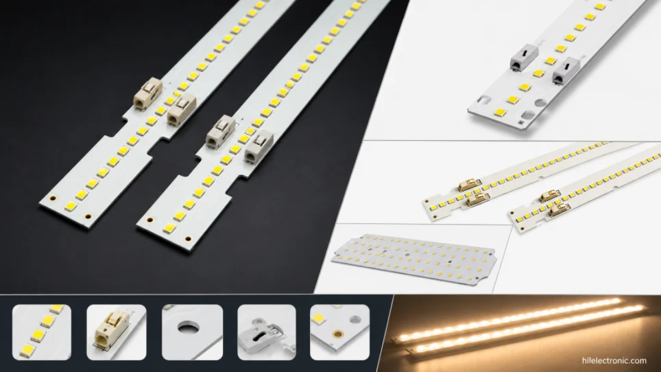
LED Linear & Strip Light PCBs: Long-Format Engines, Flexible & Rigid-Flex Boards
Figure 1. LED linear light PCB manufacturing reference....
How to get a quote for PCBs
Let‘s run DFM/DFA analysis for you and get back to you with a report. You can upload your files securely through our website. We require the following information in order to give you a quote:
-
- Gerber, ODB++, or .pcb, spec.
- BOM list if you require assembly
- Quantity
- Turn time
In addition to PCB manufacturing, we offer a comprehensive range of electronic services, including PCB design, PCBA, and turnkey solutions. Whether you need help with prototyping, design verification, component sourcing, or mass production, we provide end-to-end support to ensure your project’s success.
For PCBA services, please provide your BOM (Bill of Materials) and any specific assembly instructions. We also offer DFM/DFA analysis to optimize your designs for manufacturability and assembly, ensuring a smooth production process.