
BGA Package: Structure, Types, Design & Assembly Guide

Figure 1. BGA Packages
1. Introduction: What Is a BGA Package and Why It Matters
A BGA package (Ball Grid Array) is an IC packaging format that uses an array of solder balls on the underside of the component for electrical and mechanical connection to the PCB. Unlike peripheral-lead packages such as QFP or SOIC, a BGA package places interconnects across the entire bottom surface, enabling significantly higher I/O counts within a compact footprint.
This architecture has made the BGA package the standard choice for high-density, high-performance devices including microprocessors, FPGAs, SoCs, and advanced MCUs. The technology supports faster signal speeds, improved thermal dissipation, and greater routing density. However, these benefits come with increased demands on PCB design complexity, layer count, and assembly process control.

Figure 2. BGA Package Structure
2. Basic Structure of a BGA Package
Understanding the internal construction of a BGA package is essential for both PCB designers and process engineers. The physical architecture determines electrical performance, thermal behavior, and manufacturability.
2.1 Die (Silicon Chip)
The die is the functional silicon integrated circuit at the center of the BGA package. It contains all transistors, interconnects, and logic that define the device’s operation. The die connects to the substrate either through wire bonding from the top surface or through flip-chip bumps on the active face. Die size and power density directly influence the thermal and electrical design requirements of the package.
2.2 Substrate
The substrate is the multi-layer circuit board within the BGA package that redistributes signals from the die to the solder ball array. Common substrate materials include BT (Bismaleimide Triazine) resin and ABF (Ajinomoto Build-up Film). The substrate contains internal routing layers, microvias, and power/ground planes. Its design determines signal integrity, power delivery efficiency, and overall package reliability.
2.3 Solder Balls
Solder balls form the array of interconnects on the BGA package underside, replacing traditional peripheral leads. Ball diameters typically range from 0.3 mm to 0.76 mm depending on package pitch. Common materials include SAC305 (Sn96.5/Ag3.0/Cu0.5) for lead-free applications. The ball array pitch directly corresponds to PCB pad layout and determines fanout routing complexity.
2.4 Mold Compound
The mold compound is an epoxy-based encapsulant that protects the die and wire bonds from mechanical damage, moisture, and contamination. It also provides structural rigidity to the BGA package. Mold compound properties—including CTE (coefficient of thermal expansion), thermal conductivity, and moisture absorption—affect long-term reliability and must be matched to the substrate and die characteristics.

Figure 3. Types of BGA Packages
3. Types of BGA Packages
BGA package technology has evolved into multiple variants optimized for different performance requirements, manufacturing constraints, and application environments. Selection depends on I/O density, thermal demands, and cost targets.
3.1 Common BGA Package Variants
PBGA (Plastic BGA): The most widely used variant, featuring a laminate substrate and plastic mold compound. PBGA offers good cost-performance balance for consumer and industrial applications with moderate I/O counts.
FC-BGA (Flip-Chip BGA): Uses flip-chip die attachment with solder bumps directly connecting the die to the substrate. FC-BGA delivers superior electrical performance for high-speed processors, GPUs, and networking ASICs due to shorter interconnect paths.
CBGA (Ceramic BGA): Employs a ceramic substrate for enhanced thermal conductivity and CTE matching with silicon. CBGA is used in high-reliability applications including aerospace, military, and high-performance computing.
TBGA / μBGA / CSP-BGA: Thin and micro variants designed for space-constrained applications. CSP (Chip Scale Package) BGA approaches die size, maximizing density for mobile devices and wearables.
3.2 Differences in Pitch and Density
BGA package pitch—the center-to-center distance between adjacent solder balls—directly impacts PCB design complexity. Standard pitch options include 1.27 mm and 1.0 mm, which allow escape routing on conventional 4-6 layer boards using standard via structures.
Fine-pitch BGA packages at 0.8 mm, 0.65 mm, or 0.5 mm pitch require HDI (High-Density Interconnect) PCB technology with microvias and via-in-pad structures. Pitch selection must balance I/O requirements against PCB manufacturing capability and cost.
4. Electrical and Thermal Characteristics of BGA Packages
The area-array interconnect architecture of BGA packages provides inherent electrical and thermal advantages over peripheral-lead alternatives.
4.1 Electrical Performance
BGA package interconnects offer significantly shorter signal paths compared to leaded packages, reducing parasitic inductance and resistance. This translates to lower impedance discontinuities and improved signal integrity at high frequencies.
The distributed ground and power ball placement enables effective decoupling and return path management. These characteristics make BGA packages essential for high-speed interfaces including DDR memory, PCIe, and multi-gigabit SerDes.
4.2 Thermal Performance
The solder ball array in a BGA package creates multiple parallel thermal paths from the die to the PCB, improving heat dissipation compared to packages that rely solely on leads or exposed pads. Thermal balls—dedicated ground balls in the center array—can be connected to large copper planes for enhanced conduction.
This distributed thermal interface reduces junction-to-board thermal resistance, though high-power devices still require supplemental cooling solutions such as heatsinks or thermal vias in the PCB.

Figure 4. BGA Package vs Other IC Packages
5. BGA Package vs Other IC Packages
Comparing BGA packages against alternative formats clarifies when each technology is appropriate.
5.1 BGA Package vs QFP
QFP (Quad Flat Package) uses peripheral gull-wing leads, limiting practical I/O count to approximately 200-300 pins before the package becomes excessively large. BGA packages support thousands of I/O in a smaller footprint. QFP leads are visible and inspectable, while BGA solder joints require X-ray inspection. QFP is suitable for lower-complexity devices where visual inspection capability and easier rework are priorities.
5.2 BGA Package vs QFN
QFN (Quad Flat No-lead) packages offer a low-profile solution with exposed pad thermal performance, but I/O is limited to peripheral contacts. QFN suits moderate pin-count devices (typically under 100 pins) where height is critical. BGA packages provide superior I/O scalability and better electrical performance for high-speed signals, but require more complex PCB stackups. Both share X-ray inspection requirements for hidden solder joints.
5.3 BGA Package vs LGA
LGA (Land Grid Array) uses flat pads instead of solder balls, requiring socket mounting or careful solder paste printing. LGA simplifies component replacement in socketed applications (common for server CPUs) but demands tighter coplanarity control for direct-solder assembly. BGA packages self-align during reflow and are standard for permanent surface-mount applications.

Figure 5. Routing Challenges
6. PCB Design Considerations for BGA Packages
Successful BGA package integration requires careful attention to PCB stackup, via structures, and routing strategies.
6.1 PCB Stack-up and Layer Count
BGA packages typically require multi-layer PCBs to accommodate signal escape routing and power/ground distribution. A 1.0 mm pitch BGA may route adequately on 6-8 layers, while fine-pitch devices often demand 10+ layers with HDI construction.
The stackup must include sufficient power and ground planes adjacent to signal layers for impedance control and EMI management. Layer assignment should prioritize short via stubs and controlled impedance for high-speed signals.
6.2 Fanout Strategies for BGA Packages
Dog-bone Fanout: The standard approach uses short traces from each BGA pad to an offset via. This works well for outer rows at standard pitch but consumes routing space.
Via-in-Pad: Placing vias directly in BGA pads maximizes routing density and is often required for fine-pitch devices. Vias must be filled and planarized (VIPPO) to prevent solder wicking and ensure reliable joints.
Microvias: HDI construction with laser-drilled microvias enables fanout from inner ball rows that cannot reach standard through-hole vias. Stacked or staggered microvia structures connect multiple layers progressively.
6.3 Routing Challenges
Escape routing from high-density BGA packages requires systematic planning. Outer rows route first to inner layers, progressively freeing channels for inner rows. Critical signals (clocks, high-speed differential pairs) should be prioritized and routed on optimal layers with proper reference planes.
Power and ground balls should connect directly to planes where possible. Design rules must account for manufacturing tolerances—trace width, spacing, and via-to-pad clearances tighten significantly at fine pitch.

Figure 6. BGA Package Assembly
7. BGA Package Assembly Process Overview
BGA package assembly follows standard SMT processes with specific considerations for the hidden solder joint array.
7.1 Solder Paste Printing
Stencil design is critical for BGA package assembly. Aperture size and stencil thickness must match the ball pitch and diameter to deposit the correct solder volume. Fine-pitch BGAs typically require thinner stencils (0.10-0.12 mm) with optimized aperture ratios. Step stencils may be necessary when BGAs share a board with components requiring different paste volumes. Print quality—complete fill without bridging—directly impacts joint reliability.
7.2 Pick-and-Place and Reflow
BGA packages benefit from solder self-alignment during reflow—surface tension pulls the component into correct position even with minor placement offset. However, this requires accurate initial placement within the self-alignment window (typically ±50% of pad width).
Reflow profile optimization is essential: insufficient peak temperature causes incomplete wetting, while excessive temperature or time risks damage to moisture-sensitive components. Controlled ramp rates minimize thermal stress across the large package body.

Figure 7. BGA X-ray Inspection
8. Inspection and Reliability Concerns for BGA Packages
The hidden nature of BGA solder joints creates unique inspection and reliability challenges.
8.1 Inspection Challenges
Unlike leaded packages, BGA solder joints are not visible after assembly. Automated optical inspection (AOI) can only verify component presence and orientation. X-ray inspection is required to assess joint quality—detecting voids, bridges, head-in-pillow defects, and incomplete wetting. 2D X-ray provides basic screening; 3D computed tomography (CT) enables detailed analysis of individual joints when required for failure analysis or process qualification.
8.2 Common Failure Modes
Head-in-Pillow (HIP): Occurs when the solder ball and paste fail to fully coalesce, creating a cold joint with surface contact only. Caused by oxidation, warpage, or reflow timing issues.
Voiding: Gas entrapment within the solder joint reduces mechanical strength and thermal/electrical conductivity. Flux chemistry and reflow profile optimization minimize void formation.
Bridging and Collapse: Excessive solder volume or incorrect pad design can cause adjacent balls to bridge. Ball collapse from overheating reduces standoff height, risking shorts between package and PCB features.

Figure 8. BGA Rework for PCB Assembly
9. BGA Package Rework and Repair Considerations
9.1 Rework Difficulties
BGA package rework requires specialized equipment and operator skill. The component must be heated uniformly to reflow temperature while protecting adjacent components from thermal damage. Hot-air rework stations with component-specific nozzles and bottom-side preheating are standard. Large or high-thermal-mass BGAs demand precisely controlled temperature profiles to prevent PCB damage, pad lifting, or incomplete solder melting.
9.2 Reballing and Design Considerations
After BGA removal, PCB pads require cleaning and inspection before replacement. The replacement component may need reballing if original balls were damaged during removal. Reballing uses stencils or preforms to apply new solder balls. Design decisions can reduce rework difficulty: adequate keep-out zones around BGAs, sufficient thermal relief on pads, and avoiding placement of moisture-sensitive components nearby all improve rework success rates.
10. Typical Applications of BGA Packages
BGA packages dominate applications requiring high I/O density, high-speed signaling, or compact form factors.
10.1 Microcontrollers and Processors
Advanced MCUs, application processors, and CPUs use BGA packages to accommodate large pin counts and high-speed memory interfaces. The format supports the wide buses and multiple power domains required by modern processing architectures. Mobile application processors, automotive MCUs, and embedded SoCs commonly ship in BGA configurations.
10.2 FPGA and SoC
FPGAs and complex SoCs often exceed 1000 I/O pins, making BGA packages the only practical option. High-speed transceivers for multi-gigabit serial interfaces require the low-inductance paths that BGA architectures provide. These devices typically use fine-pitch FC-BGA packages and demand HDI PCB technology for successful implementation.
10.3 Networking and Communication Equipment
Network switches, routers, and base station equipment rely on BGA packages for ASICs and PHY devices handling high-bandwidth data. The electrical performance supports 25G/100G+ Ethernet interfaces and high-speed backplane connections. Thermal management of power-dense networking chips benefits from the distributed heat paths in BGA packages.
10.4 High-Performance Consumer Electronics
Smartphones, tablets, gaming consoles, and high-end consumer devices use BGA packages extensively. PoP (Package-on-Package) configurations stack memory BGA packages directly on processor packages to minimize footprint. The compact form factor and electrical performance enable the feature density expected in modern consumer electronics.
11. Summary: When and Why to Choose a BGA Package
The BGA package is not inherently superior to other formats—it is optimized for specific requirements. Selecting a BGA package is justified when high I/O count exceeds peripheral-lead package limits, when signal speeds demand low-inductance interconnects, or when board space constraints require maximum density.
Successful BGA implementation requires alignment between component selection and manufacturing capability. PCB layer count, via technology, and design rules must support the chosen pitch. Assembly processes need appropriate stencil design, placement accuracy, and reflow control. Inspection capability—specifically X-ray—must be available for quality verification. Rework capability should be considered during design if field serviceability is required.
The decision to use a BGA package represents a trade-off between performance advantages and increased design complexity, manufacturing requirements, and inspection costs. When application requirements align with BGA capabilities, the format delivers unmatched density and electrical performance. When simpler alternatives suffice, they may offer better overall value.

Recommended Posts
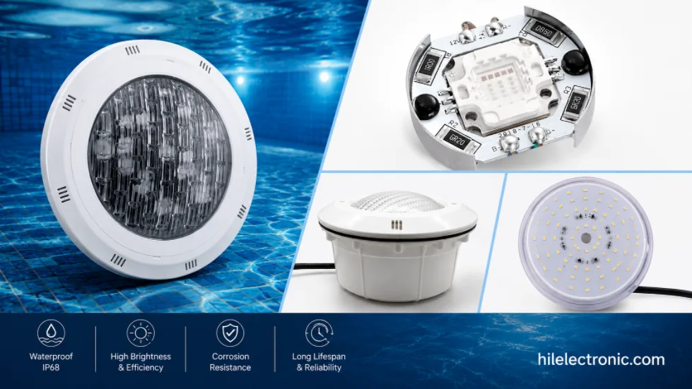
Underwater & Pool LED Light PCBs: IP68 Potted Boards, Low-Voltage Drivers & Safety
Figure 1. LED pool light PCB manufacturing reference....
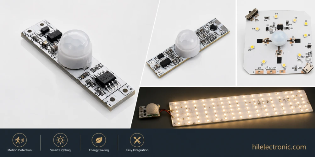
Motion Sensor & Smart LED Light PCBs: Sensor, Control, Driver & Wireless Boards
Figure 1. motion sensor LED light PCB manufacturing...

LED High Bay Light PCBs: Metal-Core Light Engines, Drivers & Turnkey Boards Built to Spec
Figure 1. LED high bay light PCB manufacturing reference....
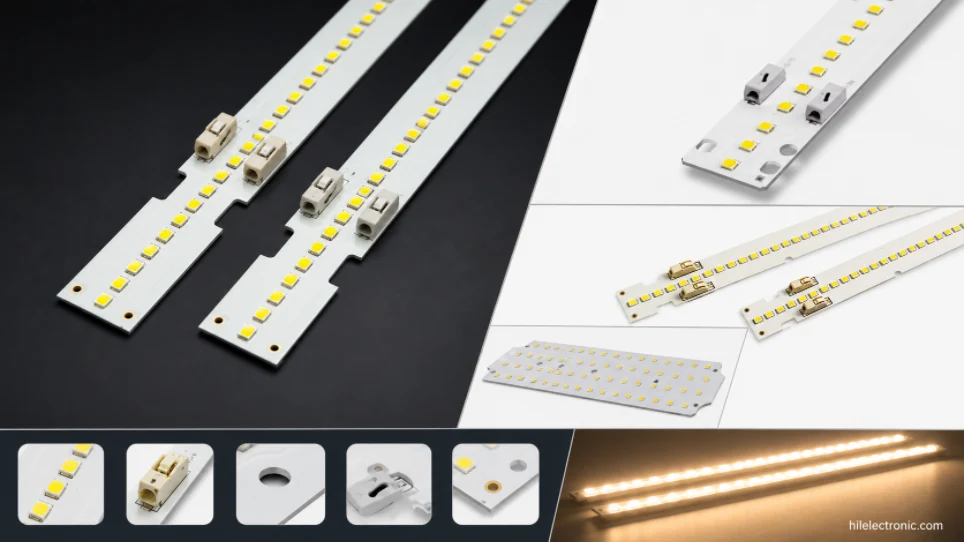
LED Linear & Strip Light PCBs: Long-Format Engines, Flexible & Rigid-Flex Boards
Figure 1. LED linear light PCB manufacturing reference....
How to get a quote for PCBs
Let‘s run DFM/DFA analysis for you and get back to you with a report. You can upload your files securely through our website. We require the following information in order to give you a quote:
-
- Gerber, ODB++, or .pcb, spec.
- BOM list if you require assembly
- Quantity
- Turn time
In addition to PCB manufacturing, we offer a comprehensive range of electronic services, including PCB design, PCBA, and turnkey solutions. Whether you need help with prototyping, design verification, component sourcing, or mass production, we provide end-to-end support to ensure your project’s success.
For PCBA services, please provide your BOM (Bill of Materials) and any specific assembly instructions. We also offer DFM/DFA analysis to optimize your designs for manufacturability and assembly, ensuring a smooth production process.