
Back to blog
A Comprehensive Guide to BGA Substrates

BGA (ball grid array) substrates have become a highly prevalent packaging technology for integrated circuits (ICs), ASICs, GPUs, and other complex components. With the ability to accommodate a high density of contacts in a small footprint, BGA enables miniaturization and performance enhancements for a wide array of electronics. However, designing with and manufacturing BGA substrates requires in-depth expertise. This comprehensive guide covers everything needed to leverage the benefits of BGA while avoiding the pitfalls.
What is a BGA Substrate?
A BGA substrate acts as the foundation for BGA packaging, providing mechanical support as well as the electrical interconnects. The substrate consists of an insulating material with conductive traces on or within it that route signals and power between the attached silicon die and the printed circuit board (PCB) on which the BGA package is mounted.
The distinguishing characteristic of all BGA packages are the small solder balls arrayed on the bottom of the package in a grid pattern. These solder balls connect the substrate traces to matching landing pads on the surface of the PCB when the BGA component is soldered to the board during assembly. This ball grid enables high density interconnects since the balls can be closely spaced.
BGA substrates must be designed specifically to match the silicon die and circuit board while also meeting electrical, thermal, and mechanical requirements. Laminates, ceramics, silicon, glass, and other materials are used to fabricate BGA substrates. The substrate design depends on factors such as the number of contacts required, signal speeds, power delivery needs, reliability expectations, and cost.
Why BGA Substrates Enable Miniaturization
The main benefits of BGA stem from the ability to fit more interconnects in a smaller space versus older IC packaging approaches. For example:
- Peripheral lead packages like quad flat packs (QFP) have leads only around the edges, limiting contact density.
- Pin grid arrays (PGA) use an array of pins extending from the bottom of the package, but minimum pin spacing is larger than solder balls.
- Leadless chip carriers have contacts on the edges or bottom, but cannot match BGA density.
By contrast, BGA can achieve very high densities with balls on a 0.5mm pitch or even 0.4mm and below. This enables more functions in smaller packages. The ideal spherical shape of the solder balls also allows closer spacing versus pins.
Higher contact counts enable integration of additional functions like multiple processors, memory, sensors, wireless, power management, and specialized accelerators within BGA packages targeted at applications like 5G, AI, ADAS, IoT, and more. The miniaturization also aligns with consumer preferences for ever more compact electronics.
Materials Used for BGA Substrates

While early BGA packages utilized ceramic substrates, newer organic substrates now predominate due to their lower cost along with advantages in thermal shock resistance, reduced warpage, and flexibility. Common materials include:
BT Substrate – Bismaleimide triazine, a thermosetting resin, typically reinforced with glass fiber and copper foil. Offers a cost-effective balance of performance and manufacturability. Widely used in consumer, telecom, industrial, and automotive applications. Withstands lead-free solder processes.
Polyimide Substrate – Provides superior thermal stability but at higher cost than BT. Used when very thin substrates are required. Common in mobile and high reliability applications.
CE Substrate – Composite epoxy resin reinforced with glass fiber. Low moisture absorption properties. Often used in high-humidity environments.
Flexible Substrate – Polyimide films can produce very thin, flexible substrates for improved shock/vibration resistance. Enables thin, compact designs.
Ceramic substrates of aluminum oxide or aluminum nitride still excel for some extremely high performance applications like aerospace where their superior thermal conductivity justifies the cost premium. Silicon or glass interposers are also emerging for very high density 2.5D/3D packages.
Why Automated BGA Substrate Design is Essential
The complexity of routing intricate escape patterns and traces from hundreds or thousands of die contacts dictates automated computer-aided design. Manual BGA substrate layout is not feasible.
Critical challenges include:
Signal Integrity – Matching trace geometries to achieve controlled, consistent impedance for every net is mandatory, along with proper reference planes for noise reduction. This requires automated optimization.
Power Integrity – Careful co-design of power and ground planes for efficient power distribution to the silicon die without excessive noise. Decoupling capacitors must also be properly placed.
Density – Escape routing from the BGA pad array demands a staggered pattern of vias and traces along with layer assignments optimized to avoid congestion and length.
Thermal – The substrate must allow sufficient heat conduction from the die to the PCB and ambient. Thermal vias help.
Reliability – Design rules for trace width/spacing, via structure, pad shapes, and materials must balance cost vs long-term robustness under temperature cycling, vibration, etc.
Only advanced EDA tools combining intricate routing algorithms, constraint managers, design rule checks, and simulation can achieve an optimal substrate design that meets the technical challenges as well as manufacturability requirements.
Key BGA Substrate Design Considerations
Here are some of the most important factors designers must consider when developing a BGA substrate:
- Signal integrity – Controlled impedance traces, proper referencing and isolation, noise mitigation, and cross-talk avoidance are critical for clean signals, especially at high speeds. This is enabled through right-angle routing, reference planes, dielectric selections, trace geometries, simulation, and length matching.
- Power integrity – Careful power plane design, decoupling capacitors, and power bump array optimizations are needed to deliver stable, low-noise power to the silicon die. Voltage drop analysis should be performed.
- Thermal management – The substrate design must enable efficient conductive and convective cooling of the die through the PCB. Thermal vias under the die are essential. High conductivity materials help.
- Reliability – Substrate and trace materials, design rules, modelling, inspection testing, and simulation help ensure robustness under temperature cycling, vibration, shock, humidity, and fatigue stresses over the product lifetime.
- Escaping – The escape routing patterns from the dense ball array to the perimeter require staggered rows of vias/traces optimized for routing density, length matching, and simplicity. HDI is often needed.
- Manufacturability – DFM practices throughout the design process ensure the substrate can be fabricated, assembled, inspected, and tested reliably at the best cost.
- Density – Higher density BGA packages demand thinner dielectrics, finer lines and spaces, smaller vias, more layers, and advanced materials to accommodate the interconnect count.
Ball Pitch in BGA Packages
Ball pitch is the distance between the centers of adjacent solder balls in the grid array. Pitch has steadily decreased to enable higher density BGA packages. Some current ball pitches include:
- 0.8mm – Widely used pitch for many cost-sensitive, medium density BGA packages
- 0.65mm – A common high density pitch for complex ICs up to about 35x35mm size
- 0.5mm – Considered an ultra fine pitch achievable with advanced PCB fabrication
- 0.4mm – An extremely tight pitch pushing the limits of manufacturing capabilities
The trend towards smaller ball pitch allows either smaller package sizes for a given interconnect count or higher densities in larger package sizes. However, shrinkage brings challenges in assembly process control, solder joint reliability, rework difficulties, and sensitivity to PCB warpage. Very fine pitch demands tight tolerances.
Key Characteristics of BGA Substrates

Some of the distinguishing features of BGA substrates that explain their advantages versus older package styles include:
- High interconnect density – The ability to concentrate 100s to 1000s of contacts in a small footprint allows integration of more functionality and I/O in a compact form factor.
- Low inductance – Minimal lead lengths between the silicon die and PCB offer superior electrical performance, especially for high frequency signals.
- Short, direct connections – The direct vertical connections eliminate fragile wire bonds and leads that can break. Reliability is higher.
- Process compatibility – BGA packages can be surface mounted like other SMT components at the PCB assembly stage, reducing costs.
- Thermal conduction – The direct die contact and short connections facilitate heat spreading into the PCB and surrounding environment, mitigating hot spots.
- Self-alignment – The surface tension of liquid solder aligns the balls with matching pads during reflow assembly. Less sensitivity to placement accuracy.
- Testability – BGA packages allow full pre-assembly testing of the encapsulated die prior to board mounting.
BGA Substrate Routing Challenges

Routing traces within or on the layers of a BGA substrate poses complex design challenges including:
Signal Integrity – Controlling trace impedance, cross-talk, and signal quality demands matching geometries, proper referencing, stubs control, phase matching, and simulation.
Power Integrity – Clean power delivery relies on low-inductance paths, adequate decoupling, proper plane isolation, thermal management, and analysis.
Routing Density – The staggered escape patterns must allow routing channels between the closely spaced rows of vias/traces exiting the dense matrix array.
Manufacturing – Design rules on trace width, spacing, shapes, vias, and materials must align with fabrication capabilities while optimizing cost and reliability.
Thermal Management – The substrate must spread heat effectively into the PCB and surrounding environment to avoid hot spots under the dense die.
Reliability – Materials, design rules, manufacturing controls, modelling, and testing help ensure the substrate will withstand stresses over the product lifetime.
Advanced EDA tools and experienced engineers are essential to address these interdependent challenges while avoiding over-design that adds unnecessary cost. The substrate development is highly interactive with continual optimization.
BGA Substrate Materials Overview
As introduced earlier, the most common materials used to fabricate BGA substrates include:
Organic Substrates
- BT (bismaleimide triazine) – Widely used due to balance of cost/performance
- Polyimide – Excellent thermal stability but higher cost
- FR-4 – Traditional glass-reinforced epoxy PCB material, lower performance/cost
- CE (composite epoxy) – Used in high humidity environments
- Flexible substrates – Polyimide or LCP films enable thin, flexing substrates
Ceramic Substrates
- Aluminum oxide (alumina) – Most common, relatively low cost ceramic
- Aluminum nitride – High thermal conductivity for very demanding applications
- Beryllia – Toxicity limits use of beryllium oxide ceramic
Other Advanced Substrates
- Silicon interposers – Enable 2.5D/3D chip stacking with TSVs
- Glass interposers – Insulating properties suited for high density interconnect
The optimal material depends on application requirements like frequency, power levels, reliability needs, dielectric properties, fabrication costs, and product lifecycles.
BGA Assembly Process Concerns
To achieve reliable solder joints during SMT assembly of BGA packages onto PCBs, certain process precautions are recommended:
- Apply adequate heat to reflow all solder balls reliably without overheating sensitive components
- Ensure even heating across the entire BGA footprint to avoid offsets in reflow that can warp the package
- Use no-clean solder paste designed for lead-free BGA assembly to avoid entrapment of residues
- Precisely control thermal profiles including ramps, soaking, and cooling
- Eliminate tombstoning through appropriate paste deposits, component centering, and profiling
- Prevent voids by applying proper paste volumes matched to ball volumes, aperture designs, and placement force
- Inspect thoroughly for indicators of poor wetting, head-in-pillow defects, non-uniformity, and other flaws
- Validate processes through design of experiments (DOE) and testing such as shear force analysis on sample joints
With fine pitch BGAs, assembly demands tighter tolerances, advanced inspection techniques, and very consistent process controls to attain high yields and reliability.
Inspecting BGA Solder Joints
Unlike more visible lead-based joints, the solder connections underneath BGAs cannot be inspected visually. Instead, X-ray imaging is the optimal solution for examining internal solder joint quality following BGA assembly.

Automated X-ray inspection (AXI) systems generate high resolution images revealing:
- Solder ball alignment, standoff height, and compression
- Presence of voids, cracks, insufficient wetting, or other flaws
- Solder ball deformation from ideal shape
- Non-uniformity between joints
- Foreign objects, contaminants, or residues
AXI provides full inspection coverage to identify assembly defects before products ship as well as potential long-term reliability risks. 3D capabilities provide further insights on the joint structure. If any defects are detected, the process can be adjusted to eliminate the root cause.
BGA Rework and Repair
If post-assembly inspections or subsequent testing reveals defects in the solder joints, component placement, or board-level interconnects associated with BGA mounting, rework will be required. Some best practices include:
- Use specialized BGA rework systems with preheaters, thermocouples, vacuum pick-up, and optical alignment
- Selectively apply focused heat only to the defective component without overheating nearby materials
- Carefully control thermal ramp up, soaking, and cooling rates throughout the re-reflow process
- Employ solder paste or flux designed for BGA rework to wet board pads reliably and avoid bridging
- Use minimum volumes of solder paste matched to pad/ball volumes to avoid excess solder
- Visually inspect for proper alignment before re-reflow; employ AXI afterwards to confirm joint integrity
- Remove all residual flux after rework using cleaners formulated for low residue
With fine-pitch BGAs, specialized tools, materials, and processes are essential for successful rework. Prevention is preferable through robust process design and control.
Advantages of BGAs
Here are some of the key benefits that have made BGA packaging pervasive across electronics:
High Density – The ability to concentrate more I/O connections in a small footprint allows integration of extra functionality and features.
High-Speed Signal Integrity – The short traces between die and board offer electrical performance advantages, especially for fast digital signals.
Reliability – Direct vertical interconnects avoid fragile wire bonds and leads prone to breakage from thermal or mechanical stresses.
Thermal Performance – Direct die contact and short connections promote heat conduction away from the dense, hot silicon into the PCB and surrounding ambient air.
Design Flexibility – A wide range of substrate materials with various dielectic properties can be selected to meet technical and cost requirements.
Testability – Known-good die can be fully tested encapsulated in BGA packages prior to board assembly for improved yields.
Process Compatibility – BGA packages can be surface mounted like other SMT components, leveraging high volume PCB assembly.
Limitations of BGA Packages
Despite significant benefits, BGAs also come with some limitations and tradeoffs:
Inspectability – The inability to visually examine internal solder joints means X-ray inspection is required to verify assembly integrity.
Rework Difficulty – Removing and replacing BGAs without damaging boards or adjacent components requires advanced tools and skills.
Board Warpage Sensitivity – Thermal stresses can warp boards enough to break connections to easily distorted solder balls under large BGAs.
Cost – High density interconnect fabrication and advanced substrate materials drive cost above older package styles with lower contact counts.
Signal Routing Congestion – Very high I/O count BGAs require multiple, dense routing layers and complex escape patterns that add PCB fabrication expense.
Second Level Interconnect – A separate assembly stage is required to attach the die onto the BGA substrate prior to board mounting.
Thermal Stress – CTE mismatches between silicon, substrate, board, and solders must be considered to avoid temperature cycle failures.
BGA Substrates vs. LGA
Land grid array (LGA) packages offer an alternative to BGA with some distinct tradeoffs:
Removability – LGAs use land pads rather than solder balls, allowing insertion/removal from socket connectors on PCBs. BGAs are permanently soldered.
Reliability – LGAs avoid solder fatigue failure modes, but the many socket interconnects are less reliable than solder joints under thermal cycling.
Rework – Defective LGAs can be detached and replaced without desoldering or board heating. BGAs require re-reflow.
Contact Wipe – LGA pads rub on connector pins during insertion, removing oxidation and debris for low contact resistance. BGAs rely on soldering alone.
Routing – LGAs demand high densities of plated through holes and vias for the socket pins while BGAs require escape routing for traces.
Profiles – LGA stands taller than BGA by at least the socket height. BGA provides a lower profile.
Cost – For high volume production, BGA is generally lower cost. LGA may be preferred for moderate volumes.
The optimal choice depends on cost targets, lifecycle expectations, field servicing needs, and performance requirements.
BGA Applications Across Industries
The high performance, small size, and reliability of BGA packages has seen adoption across a wide range of applications:
Consumer Electronics
- Smartphones, tablets, laptops
- Gaming consoles, set-top boxes
- Digital cameras, wearables
Automotive
- Engine control units, infotainment
- ADAS modules, LiDAR
- Body controllers
Aerospace and Military
- Avionics computer boards
- Radar and imaging systems
- Missile guidance systems
Telecom and Networking
- Switches, routers, base stations
- Servers
- Fiber optics modules
Medical
- Imaging systems like MRI, CT, PET scanners
- Patient monitors and diagnostics
- Implantables like pacemakers
Conclusion
As this guide has illustrated, BGA substrates require thoughtful engineering across numerous disciplines – electrical, thermal, mechanical, materials science, physics, manufacturing, and more.
When designed properly, BGA substrates provide a high reliability interconnection method enabling continued technological advances. But they require careful modeling, analysis, adherence to sound design practices, and tight process controls to achieve product quality and reliability goals.

Recommended Posts

Clean Flux vs No-Clean Flux: Residue, Cleaning, and PCB Reliability
Figure 1. clean flux vs no-clean flux image for Highleap...
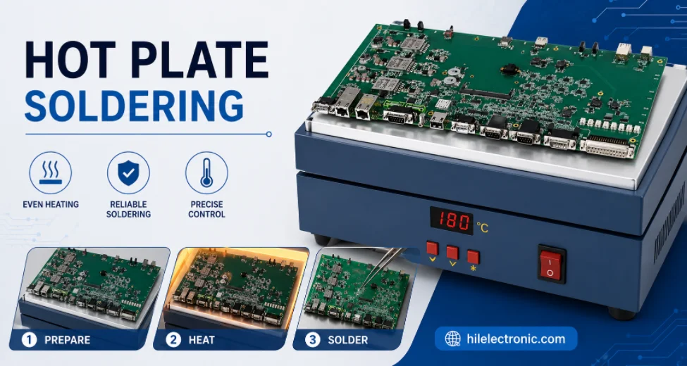
Hot Plate Soldering: Process, Limits, and Reflow Comparison
Figure 1. hot plate soldering image for Highleap...
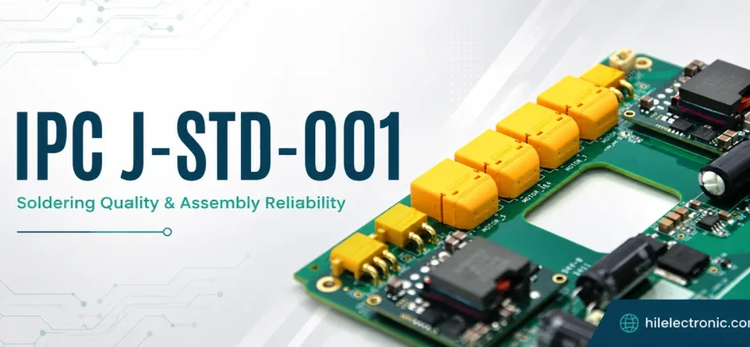
IPC J-STD-001: Classes, Requirements, and RFQ Specification
Figure 1. IPC J-STD-001 image for Highleap Electronics PCB...
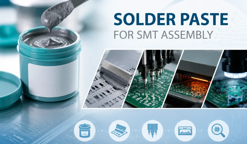
Solder Paste for SMT Assembly: Types, Storage, and Printing Defects
Figure 1. Solder paste selection affects SMT print...