
How to Solder Wires to a Circuit Board: A Step-by-Step Practical Guide

1. Overview
Soldering wires to a circuit board is a fundamental skill for creating reliable electrical and mechanical connections. Whether you are working on DIY electronics, performing repairs, or building prototypes, mastering wire-to-PCB soldering ensures signal integrity and long-term durability. This guide provides a systematic approach to soldering wires to PCBs correctly, covering preparation, core techniques, quality assessment, and common troubleshooting methods.
The primary challenges in wire-to-board soldering include managing flexible conductors, controlling heat application, and avoiding defects such as cold joints or solder bridges. Understanding these factors before starting will significantly improve your results. The following sections progress logically from foundational concepts through detailed procedures to inspection and problem-solving.
2. Fundamentals of Wire-to-PCB Soldering
Before proceeding to the hands-on steps, understanding the underlying principles helps ensure that each action serves a clear purpose. This section explains what wire-to-PCB soldering accomplishes and the thermal dynamics involved.
2.1 What Is Wire-to-PCB Soldering
Soldering a wire to a circuit board forms both an electrically conductive path and a mechanical bond. Molten solder alloy wets the surfaces of the wire strands and the PCB pad, then solidifies to lock the connection in place.
Two primary methods exist: through-hole soldering, where the wire passes through a plated hole and is soldered on the opposite side, and surface soldering, where the wire is attached directly to a surface-mount pad. Through-hole connections offer stronger mechanical support, while surface soldering suits boards without pre-drilled holes or high-density SMT layouts.
2.2 Solder and Heat Principles
Temperature control is critical when you solder wires to a circuit board. Solder must reach its melting point to flow properly, yet excessive heat can damage the PCB laminate or lift pads. Capillary action draws molten solder into microscopic gaps between surfaces, a process called wetting. Good wetting produces shiny, smooth joints.
Insufficient heat causes cold joints—grainy, dull connections with poor conductivity. Excessive solder or careless iron placement can create solder bridges that short adjacent traces. Recognizing these outcomes guides proper technique.
3. Tools and Materials for Soldering Wires to a Circuit Board
Gathering the correct tools and materials before starting reduces errors and improves efficiency. This section lists essential and optional items along with their purposes.
3.1 Essential Tools
- A temperature-controlled soldering station is the most important tool; adjustable settings between 330°C and 380°C accommodate different solder types.
- Use rosin-core solder wire in an appropriate alloy—leaded (60/40 or 63/37) or lead-free (RoHS-compliant SAC305)—with matching flux.
- Wire strippers sized for your conductor gauge, fine-tip tweezers, and a third-hand fixture or PCB holder keep components stable during soldering.
- Cleaning supplies such as isopropyl alcohol, lint-free wipes, and a brass tip cleaner or damp sponge maintain iron tip condition.
3.2 Optional Aids
- Heat-shrink tubing or silicone sleeves provide strain relief and insulation after soldering.
- A magnifying lamp or stereo microscope assists with visual inspection of fine-pitch work.
- Desoldering braid (solder wick) and a vacuum desoldering pump enable rework if joints require correction.
These items are not mandatory but improve quality and convenience.
3.3 Material Preparation
Select wire gauge based on current requirements—thicker conductors for higher currents. Strip insulation to expose approximately 3–5 mm of conductor, then twist stranded wire tightly to prevent splaying. Pre-cutting wires to length and organizing them before soldering streamlines the process.

4. Step-by-Step Guide: How to Solder Wires to a Circuit Board
This section details each stage of the soldering process in practical sequence. Following these steps consistently produces strong, reliable connections.
4.1 Step 1 — Clean and Prepare Surfaces
Oxides and contaminants prevent proper wetting. Wipe the PCB pads with isopropyl alcohol to remove residue. If the wire ends show tarnish, lightly abrade them or apply flux. Clean surfaces accept solder more readily and produce stronger joints.
4.2 Step 2 — Pre-Tin the Wire and Pad
Pre-tinning applies a thin solder layer to each surface before joining them. Heat the exposed wire end and feed solder until the strands absorb a small amount. Repeat on the PCB pad. Pre-tinning improves thermal transfer and accelerates the final joint formation, reducing overall heat exposure to the board.
4.3 Step 3 — Secure the Wire and PCB
Movement during soldering causes cold joints. Clamp the PCB in a holder and position the wire using a third-hand tool or tape. For through-hole connections, insert the wire, bend it slightly on the underside to hold it in place, then secure the board. Stability is especially important for thick or long wires that conduct heat away quickly.
4.4 Step 4 — Heat Both Surfaces Simultaneously
Place the soldering iron tip so it contacts both the wire and the pad at the same time. This ensures both reach working temperature together. Hold for one to two seconds—long enough to transfer heat, short enough to avoid damage. Consistent contact angle and pressure improve heat flow.
4.5 Step 5 — Apply Solder and Form the Joint
Feed solder wire to the heated junction—not directly to the iron tip. Capillary action draws the molten solder around the wire and across the pad. Add just enough to create a concave fillet; excessive solder increases the risk of bridges. A properly formed joint appears shiny and smooth with a slight meniscus shape.
4.6 Step 6 — Cool and Clean
Remove the solder wire first, then lift the iron away. Allow the joint to cool naturally without blowing or movement. Trim excess wire leads flush without stressing the solder. Finally, clean flux residue with isopropyl alcohol to prevent corrosion and improve inspection visibility.
5. Quality Inspection and Testing
Verifying each solder joint ensures the circuit board will function reliably. A brief inspection routine catches defects before they cause failures.
5.1 Visual Inspection
Examine each joint under good lighting or magnification. Acceptable joints are shiny, smooth, and free of cracks or voids. Check that solder has not bridged to adjacent pads or traces. Dull, grainy, or blobby joints indicate potential cold solder or insufficient wetting.
5.2 Electrical Testing
Use a multimeter in continuity mode to confirm a low-resistance path between the wire and the intended circuit node. If the meter does not beep or shows high resistance, the joint may be defective. Also check for unintended shorts to neighboring connections.
5.3 Common Defects Reference
The following table summarizes typical soldering defects, their causes, and corrective actions.
| Defect | Cause | Corrective Action |
|---|---|---|
| Cold Joint | Insufficient heat or movement during cooling | Reheat joint fully; keep steady while cooling |
| Solder Bridge | Excess solder connecting adjacent pads | Remove with desoldering braid; use less solder |
| Insufficient Wetting | Oxidized surfaces or inadequate flux | Clean surfaces; apply fresh flux before re-soldering |
| Lifted Pad | Excessive heat or mechanical stress | Repair trace if possible; prevent with lower temp and care |
| Solder Balls | Flux spatter or contamination | Use proper temperature; ensure clean flux |
6. Troubleshooting Common Problems When Soldering Wires to Circuit Boards
Even experienced technicians encounter issues. Identifying root causes quickly minimizes rework time.
6.1 Typical Defects During Soldering
Cold joints result from insufficient heat or movement during cooling; they appear dull and feel weak. Solder bridges form when excess solder connects adjacent pads—common on fine-pitch boards. Solder balls occur when flux spatters; proper temperature and fresh solder reduce them. Lifted pads happen when excessive heat or mechanical force breaks the adhesive bond between the copper and substrate.
6.2 Rework Techniques
To remove excess solder, press desoldering braid onto the joint while heating from above; capillary action wicks solder into the braid. A desoldering pump can extract larger amounts quickly. When re-soldering, apply fresh flux to improve flow. Work methodically to avoid compounding damage.
7. Safety Precautions
Soldering involves high temperatures and chemical fumes. Following basic safety practices protects your health and equipment.
Work in a well-ventilated area or use a fume extractor to avoid inhaling flux vapors. Wear safety glasses to protect against solder splashes. Keep the iron in a stable stand when not in use to prevent burns or fire. Use an ESD wrist strap and grounded mat when handling sensitive components. Maintain a clean, organized workspace to reduce accidents.
8. Summary
Successfully soldering wires to a circuit board depends on proper preparation, controlled heat application, and systematic inspection. Clean surfaces and pre-tinning establish the foundation; stable fixturing and simultaneous heating of wire and pad produce sound joints. Visual and electrical tests confirm quality, while understanding common defects enables efficient troubleshooting. With practice, these techniques become intuitive, leading to reliable connections in any electronics project.

Recommended Posts
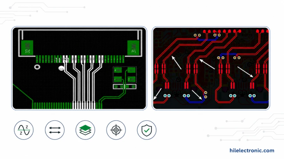
10 Layer PCB Impedance Control and TDR Verification
Figure 1. 10 layer PCB impedance control coupon and TDR...
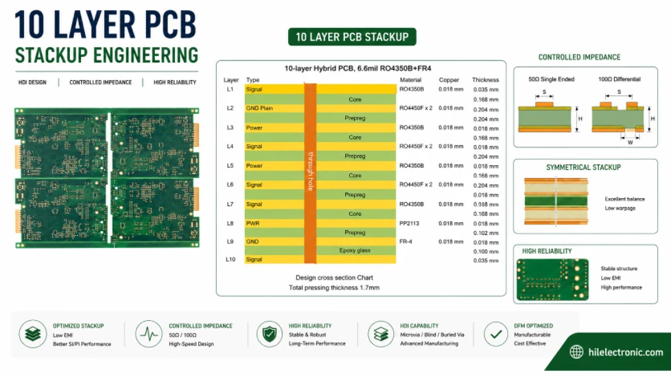
10 Layer PCB Stackup Design for Impedance and Planes
Figure 1. 10 layer PCB stackup for impedance and plane...
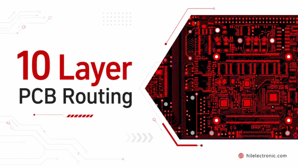
10 Layer PCB Routing Rules for DDR5, PCIe and Crosstalk
Figure 1. 10 layer PCB routing rules for DDR5 PCIe and...
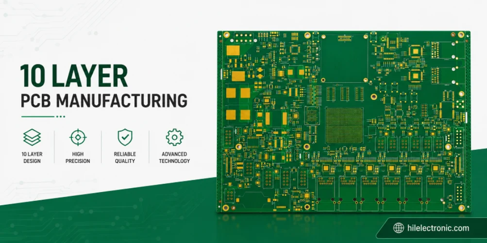
10 Layer PCB Manufacturer for Rigid, Flex and Rigid-Flex
Figure 1. 10 layer PCB manufacturer production capability....
How to get a quote for PCBs
Let‘s run DFM/DFA analysis for you and get back to you with a report. You can upload your files securely through our website. We require the following information in order to give you a quote:
-
- Gerber, ODB++, or .pcb, spec.
- BOM list if you require assembly
- Quantity
- Turn time
In addition to PCB manufacturing, we offer a comprehensive range of electronic services, including PCB design, PCBA, and turnkey solutions. Whether you need help with prototyping, design verification, component sourcing, or mass production, we provide end-to-end support to ensure your project’s success.
For PCBA services, please provide your BOM (Bill of Materials) and any specific assembly instructions. We also offer DFM/DFA analysis to optimize your designs for manufacturability and assembly, ensuring a smooth production process.