
Back to blog
Understanding and Preventing Solder Balls on PCBs: A Comprehensive Guide

Solder Balls
Soldering is a fundamental process in electronic manufacturing, crucial for creating reliable electrical connections on PCBs. However, despite its importance, soldering can sometimes lead to defects, with solder balls being a common issue encountered in SMT assembly processes.
What Are Solder Balls?
Solder balls are unintended spherical beads of solder that form during the reflow soldering process. These tiny balls can appear around component leads, on PCB pads, or within the circuit board itself. While small in size, solder balls pose significant risks to the functionality and reliability of electronic devices.
Causes of Solder Balls
The formation of solder balls can be attributed to various factors related to both materials and assembly techniques:
Material Causes:
- Solder Paste: Issues such as low activity temperature, excessive flux, uneven metal particles, or oxidized tin powder can contribute to solder ball formation.
- PCB Pads: Poor solderability of components or inadequate spacing between pads can also lead to solder ball issues.
- Stencil Quality: Dirty or damaged stencils with burrs can introduce contaminants that cause solder balls during the paste application process.
- Scraping Blade: Improperly designed or worn-out scraping blades can inadvertently cause solder to accumulate and form balls during stencil cleaning.
Technological Causes:
- Soldering Parameters: Incorrect temperature profiles, excessive pressure during component placement, or improper paste application techniques can all promote solder ball formation.
- Environmental Factors: High humidity levels and inadequate storage conditions can introduce moisture, affecting solder paste consistency and leading to solder ball defects.
Understanding the Benefits of Solder Balling for PCB Designers
Effective management of solder ball issues not only enhances product reliability but also offers several benefits to PCB designers and electronic device manufacturers. By reducing the incidence of solder ball defects:
- Enhanced Product Quality: Minimizing solder ball defects leads to higher-quality PCBs with improved electrical performance and mechanical reliability, meeting stringent industry standards and customer expectations.
- Cost Savings: Preventing solder ball defects reduces the need for rework and lowers production costs associated with scrap materials and labor-intensive troubleshooting processes.
- Increased Operational Efficiency: Streamlined manufacturing processes result in faster time-to-market for electronic products, enabling manufacturers to respond swiftly to market demands and gain a competitive edge.
For further insights into PCB manufacturing and troubleshooting, Highleap Electronic remains committed to supporting your needs with expert guidance and tailored solutions. Partner with us to leverage our industry expertise and comprehensive resources for optimal PCB performance.
Impact of Solder Balls on PCBs
The presence of solder balls can compromise the performance and reliability of PCBs in several ways:
- Electrical Performance: Solder balls can create unintended electrical connections or shorts between neighboring components, potentially causing circuit malfunction or failure.
- Mechanical Reliability: If dislodged, solder balls can migrate across the PCB surface, causing intermittent electrical connections or physical damage to sensitive components.
- Aesthetic Quality: Visible solder balls can detract from the visual appeal of electronic products, impacting consumer perception and product quality.
Preventive Measures
To mitigate the occurrence of solder balls and ensure high-quality PCB assemblies, consider implementing the following preventive measures:
- Optimized Solder Paste: Select solder paste formulations that match PCB pad specifications, ensuring compatibility in terms of metal alloy composition and flux activity.
- Stencil Maintenance: Regularly inspect and clean stencils to remove debris and ensure uniform paste deposition during the assembly process.
- Temperature Control: Maintain precise control over reflow soldering temperatures to prevent excessive oxidation or thermal expansion that can lead to solder ball formation.
- Humidity Control: Store PCBs and soldering materials in a controlled environment with low humidity levels to minimize moisture absorption and its detrimental effects on solder paste consistency.
- Process Validation: Conduct thorough process validations and quality checks throughout the PCB assembly process to identify and rectify potential sources of solder ball defects.

BGA solder joint and solder ball inspection
Conclusion
Overall, while soldering is essential for creating reliable electrical connections in PCB assemblies, solder balls represent a common defect that can compromise product quality and reliability. By understanding the causes of solder balls and implementing proactive preventive measures, manufacturers can minimize the occurrence of these defects and ensure the consistent production of high-quality PCBs.
A deep understanding of solder balls allows PCB designers to refine their design methodologies to meet stringent reliability standards. By focusing on reducing solder ball defects, designers can enhance the overall quality and durability of electronic products. This not only improves product performance but also enhances customer satisfaction by delivering PCBs that consistently meet or exceed industry expectations for reliability and functionality. In essence, incorporating insights into solder ball formation into PCB design strategies empowers designers to create more resilient and high-performance electronic devices.
For further insights into PCB manufacturing and troubleshooting, Highleap Electronic remains committed to supporting your needs with expert guidance and tailored solutions. Partner with us to leverage our industry expertise and comprehensive resources for optimal PCB performance.
For a more complete production review, use this article alongside heavy copper board production and PCB overcurrent protection when checking stackup, assembly, or test requirements.
FAQ
- How does the composition of solder paste affect the formation of solder balls on PCBs?The composition of solder paste, including the type and size of metal particles and the flux activity, can influence the propensity for solder ball formation during reflow soldering. Variations in particle distribution or flux chemistry may lead to different surface tension behaviors, impacting the formation and size of solder balls.
- Can the design of PCB vias contribute to solder ball defects?Yes, the design of vias, particularly their size and positioning relative to component pads, can affect solder ball formation. Vias that are too close to pads or poorly plated can trap solder during reflow, potentially forming solder balls as the solder reflows and moves through the via structure.
- How does the surface finish of PCBs influence solder ball formation?The surface finish of PCBs, such as HASL (Hot Air Solder Leveling), ENIG (Electroless Nickel Immersion Gold), or OSP (Organic Solderability Preservatives), can impact solder ball formation. Each finish has unique properties affecting solder wetting and flow behavior during reflow, which in turn can influence the likelihood of solder ball defects.
- What role does solder mask thickness play in preventing solder ball defects?Solder mask thickness is critical in PCB manufacturing as it affects the amount of solder paste deposited and the release of trapped gases during reflow. An inadequate solder mask thickness can lead to uneven heating and outgassing, potentially contributing to the formation of solder balls in areas with poor paste release.
- How can the alignment of PCB components during reflow soldering impact solder ball formation?The alignment of components on the PCB during reflow soldering can influence solder ball formation. Misalignment or uneven placement of components may cause uneven distribution of solder paste, leading to variations in surface tension and potential solder ball formation at critical points on the PCB assembly.

Recommended Posts
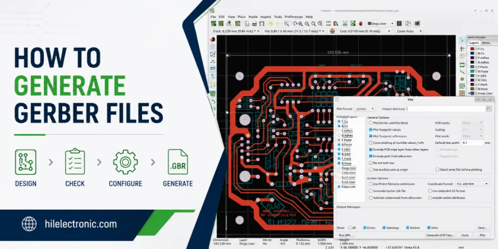
How to Generate Gerber Files for PCB Manufacturing
Figure 1. how to generate Gerber files image for Highleap...
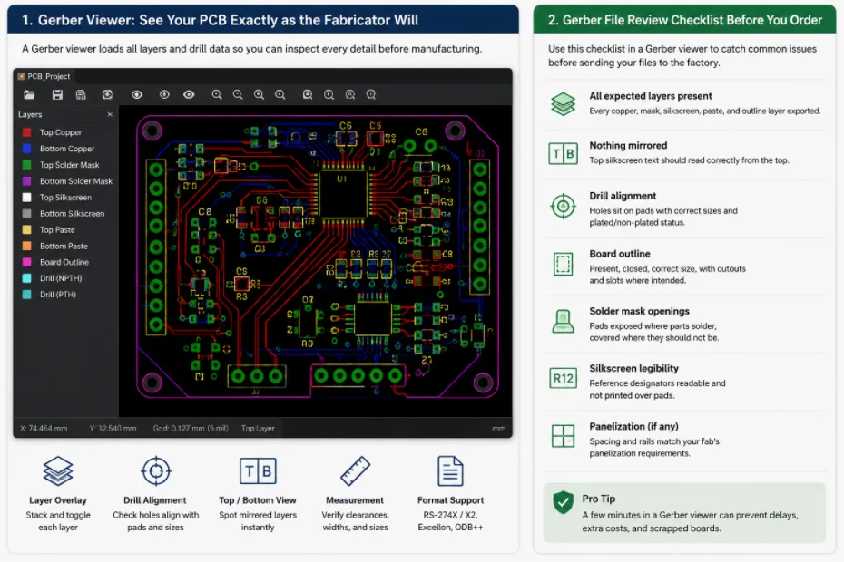
Gerber File Review Checklist: How to Check PCB Files Before You Order
Figure 1. Gerber file review catches missing layers, drill...
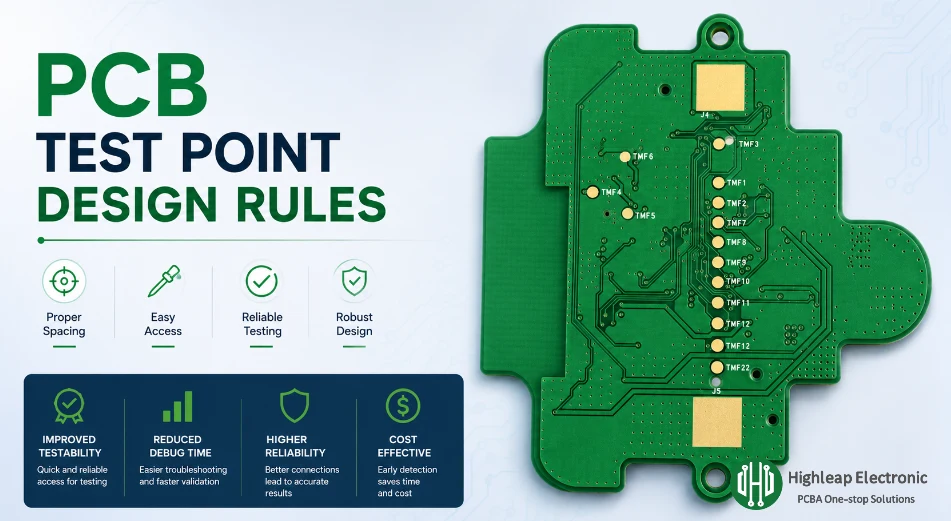
PCB Test Point Design Rules for Debug and ICT
Figure 1. PCB test point design rules help make debugging,...
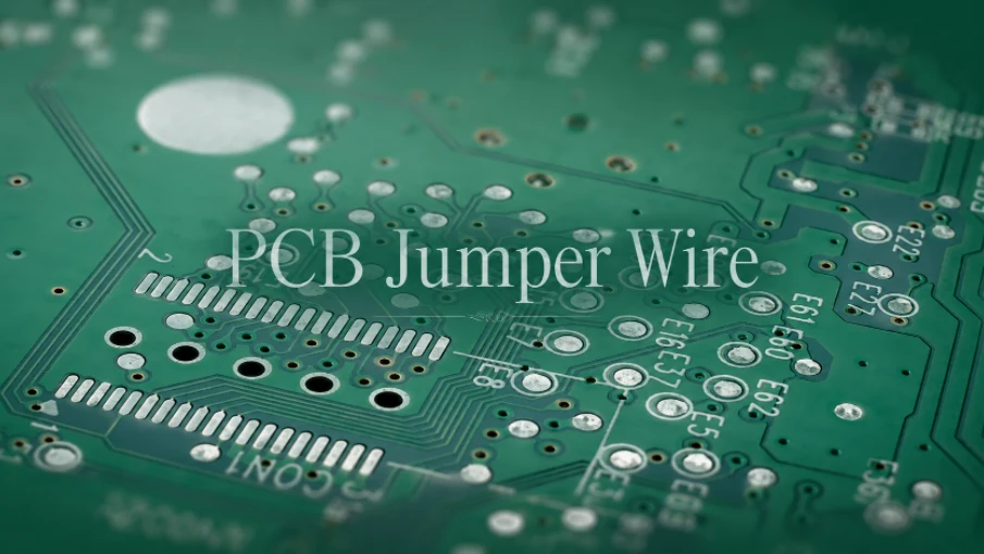
PCB Jumper Wire: Uses, Types, and Design Tips
Figure 1. PCB jumper wires are useful for prototypes and...
Take a Quick Quote