
Arlon 35N PCB Manufacturing and Polyimide Lamination
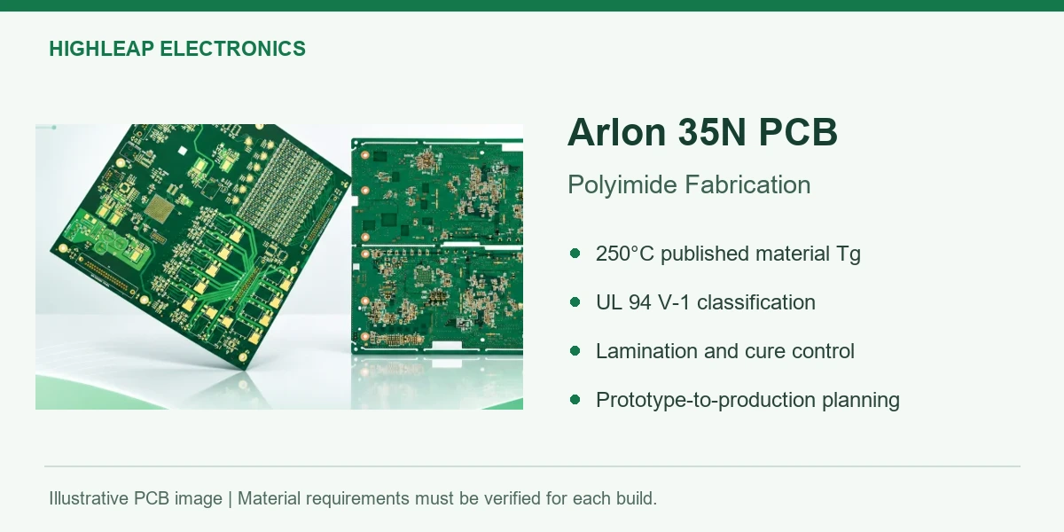
PCB manufacturing illustration. Confirm the specified Arlon material grade through the project documentation and material traceability.
Arlon 35N PCB fabrication is a process-window problem: how to produce a repeatable polyimide multilayer through material preparation, controlled cure, drilling, plating and assembly transfer. Arlon describes 35N as a flame-retardant polyimide system with a reduced cure cycle relative to traditional polyimides. That does not mean it can be run as ordinary FR-4, nor that it automatically cures faster than Arlon 33N. Both grades have a similarly described 90-minute final cure hold in their published processing guidance.
For Highleap Electronics, the useful task is to review an OEM’s 35N construction for manufacturability, supply, inspection and, where requested, PCB assembly. A technically reliable quote states the intended material and process boundaries before making delivery promises. When quoting Arlon 35N PCB prototypes or repeat orders, the process review should show how pilot-build evidence can be carried forward without assuming that the material guarantees a shorter factory lead time.
Arlon 35N PCB — At a Glance
The supplier describes reduced cure versus traditional polyimide cycles—not a universal advantage over Arlon 33N. Final cure and factory cycle time must be confirmed for each construction.
The Correct Reason to Specify 35N
Arlon’s current polyimide listing identifies 35N as a 250°C Tg flame-retardant polyimide, with 1.2% Z-axis expansion over 50–260°C, 407°C decomposition at 5% weight loss and UL 94 V-1. The manufacturer positions its cure behavior as shorter or less demanding than that of traditional polyimide systems, making it relevant where thermal reliability and manufacturing cycle time both matter.
The engineering choice should begin with the actual project constraints. A densely drilled multilayer board can be vulnerable to plated-hole thermal fatigue; a thick, copper-heavy construction can create resin-flow and registration difficulties; a repeat OEM order may be sensitive to material-lot and process variation. 35N’s resin system can be a candidate, but none of those issues disappears simply because the material has a high Tg.
Table: swipe horizontally on narrow screens to view all columns.
| Decision dimension | 35N information | What must still be defined on the board |
|---|---|---|
| Resin system | Flame-retardant polyimide laminate/prepreg | Required dielectric construction and material approvals |
| Tg | 250°C | Actual operating-temperature, thermal-cycling and assembly requirements |
| 5% decomposition temperature | 407°C | Separate from permitted solder/reflow profile and long-term service rating |
| Z-axis expansion | 1.2%, 50–260°C | Hole geometry, copper plating and board-specific thermomechanical risk |
| Flame classification | UL 94 V-1 | Whether the OEM requires this grade or a specific V-0 construction |
| Supplier positioning | Reduced cure relative to traditional polyimide | Whether the facility’s qualified process and panel mix realize a scheduling benefit |
A key qualification is that Arlon 33N is listed V-0, whereas 35N is V-1. Material substitution is not justified by a shared Tg or slash-sheet designation alone. The approved PCB material specification governs permitted changes, and the product’s own safety or reliability approvals may impose additional restrictions.
Selection boundary: If the OEM requires the specifically approved 33N construction or V-0 material flame classification, 35N’s V-1 listing must be treated as a design and documentation change. If the requirement allows a different polyimide, the decision still needs a review of thermal properties, prepreg availability, processing and qualification—not simply a comparison of 250°C Tg values.
Build a Lamination Window Around the Product Temperature, Not a Stopwatch
The value of a resin’s shorter cure concept can be lost if the board shop interprets a published hold time without accounting for panel temperature, lay-up thickness and copper balance. Arlon’s 35N product guidance specifies prepreg storage around 60–70°F (approximately 16–21°C) at ≤30% relative humidity, with 8–12 hours vacuum desiccation before lay-up. It describes baking inner layers for 60 minutes at 107–121°C directly before lay-up, a 30–45-minute pre-vacuum and controlled heating around 4.5–6.5°C/min through 100–150°C.
For the published final cure approach, the press is set around 213°C and the 90-minute hold begins once the product reaches approximately 210°C. The specified cooling under pressure also matters. These are supplier reference conditions; qualified factory settings and acceptance criteria must be established for the actual construction rather than copied verbatim into every production traveler.
A 90-minute hold is only one part of the press cycle
Record prepreg exposure, vacuum desiccation and inner-layer preparation.
Control the specified ramp and begin the hold using the product-temperature criterion.
Record cooling, thickness, registration and material-related anomalies.
Why a 90-minute hold does not equal a 90-minute press cycle
Suppose the laminate enters the critical heating range at 100°C. At an illustrative 5°C/min, the 100→150°C interval takes (150 − 100) / 5 = 10 minutes. That is only one segment of the press cycle. Preparation, pre-vacuum, the remainder of the heating ramp, time required for the actual panel to reach cure temperature, cool-down and unloading all add time. A material described as having reduced cure relative to older polyimides does not justify quoting a universally shorter board lead time from the hold number alone.
This is particularly important in multilayer PCB production, where thick panels and copper-rich areas may not follow the same temperature history as a thin test laminate. Production planning should establish which measurements represent the slowest-heating region and which deviations trigger additional engineering review.
What a process-window qualification should record
- Incoming condition: material designation, lot, core and prepreg type, storage history and traceability.
- Lay-up condition: inner-layer surface treatment, humidity control, material preparation and actual elapsed time before press loading.
- Thermal history: heat-up rate in the stated interval, product-temperature arrival at cure and held duration, cool-down and press record.
- Resulting construction: pressed dielectric thickness, panel movement, registration, bond quality and cross-section evidence in the most demanding copper-pattern region.
- Change boundaries: material-lot or prepreg-construction changes, copper-distribution changes, new panel thickness or revised equipment that may require re-qualification.
Simply recording that ‘lamination passed’ is weak evidence when the OEM expects repeatability across pilot and production orders.
Hole Formation, Copper Interfaces and Failure Diagnosis
After lamination, 35N must still be drilled, desmeared and plated. A high-Tg resin does not eliminate drill smear or copper junction defects. The supplier’s reference material lists around 350 SFM for drilling, with guidance for small via tools, and permits polyimide-compatible alkaline-permanganate or plasma desmear. Actual RPM and peck or stack parameters are derived from tool size and board geometry, not copied as one fixed setting.
Separate the symptoms before choosing a corrective action
A defective via may fail electrical test, but the root cause could lie upstream. For example, if a cross-section reveals insulating resin over inner copper, increasing final plating time will not reliably fix the original exposure problem. If the hole is mechanically rough and resin is fractured, a more aggressive desmear may worsen rather than correct the interface. If the junction is clean but copper deposition is discontinuous, the process investigation moves to activation and plating coverage.
Table: swipe horizontally on narrow screens to view all columns.
| Defect evidence | Primary question | Manufacturing lever to investigate |
|---|---|---|
| Resin smear over inner-layer pad | Was drilling followed by sufficient dielectric removal? | Drill tool condition and qualified polyimide desmear |
| Excessive dielectric recession | Was the hole wall over-attacked or damaged? | Desmear strength/exposure and drilling damage |
| Voids or thin copper in barrel | Was metallization continuous through the whole hole? | Activation, solution access and plating distribution |
| Cracks after heat exposure | Is the failure copper fatigue, weak junction or laminate separation? | Hole geometry, plating quality and thermal history |
| Bow/twist after pressing | Is the stack-up asymmetric or compaction uneven? | Copper balance, lay-up symmetry and press process |
For an OEM, this provides a better inspection conversation than saying ‘100% electrical test ensures reliability.’ Electrical test verifies defined connectivity/isolation at the time of test; it may not reveal a latent plated-hole weakness under thermal cycling. The PCB inspection plan should determine whether coupons, microsections, thermal-stress tests or other product-specific evidence is needed, and at what production stage.
A Real Pilot Build Should Challenge the Process, Not Just Produce Working Boards
If a 35N design is new to the factory or involves unusually dense via fields, large copper imbalances or additional pressing stages, the most informative pilot is one that checks the sensitive manufacturing boundaries. A first-article pass establishes a baseline, but it is not the same as demonstrating repeatability.
An illustrative process-verification plan
- Select representative panels and coupons. Include high copper, sparse copper, thick sections and the smallest or deepest relevant holes. Use OEM-approved drawings and acceptance criteria.
- Record input variation. Distinguish material lots, prepreg construction, panel loading and equipment condition rather than combining all panels into a single untraceable pass/fail group.
- Inspect before defects become inaccessible. Check pressed thickness and registration after lamination; inspect hole-wall condition and plating on coupons where the process risk warrants it.
- Verify the completed board. Use the agreed electrical and dimensional checks, with microsections or thermal evidence when required by the acceptance plan.
- Compare pilot and repeat lots. Trend measurable values such as thickness, registration, hole copper or dimensional stability; investigate shifts before they become field problems.
Define measurable pilot-build gates
On smaller screens, swipe the table horizontally to view all columns.
| Qualification gate | Evidence to retain | Escalation trigger |
|---|---|---|
| Input controls | Lot, resin/prepreg callout, storage and lay-up history | Material or condition outside approved drawing and traveler |
| Press process | Representative product-temperature history and registered panel dimensions | Thermal or registration excursion outside qualified limits |
| Mechanical interconnect | Hole-wall sections, copper connection quality and agreed thermal tests | Smear, junction defects, barrel weakness or nonconforming results |
| Repeatability release | Multiple representative builds or lots when required; documented acceptance comparison | Variation that cannot be explained or held within the approved window |
No fabricated yield numbers or machine-control limits are assumed here. The point is methodological: qualification is stronger when a repeat production plan is linked to the known sources of variation. A useful PCB manufacturer’s answer is a list of which risks are being controlled and how they will be observed, not an unsupported claim that the factory always achieves zero defects.
Arlon 35N PCB Fabrication: PCB-to-PCBA Handoff and RFQ
35N’s thermal properties do not set the acceptable reflow conditions of connectors, BGAs, adhesives, batteries or other assembled components. The final PCBA process must respect the solder alloy, surface finish, component specifications and planned number of heating cycles. Board moisture management may also be important when a high-temperature board has been stored before assembly. PCB assembly acceptance should therefore be defined separately from bare-board material-property acceptance.
A complete 35N request should include fabrication files, stack-up, thickness/copper weights, precise core/prepreg callout, drilled/finished holes and any buried-via stages, impedance and tolerances, flame requirement, acceptance class and tests, quantities, timing and approved-substitution rules. For PCBA, provide BOM, placement, solder and inspection details plus the required functional tests. The factory should confirm material sourcing, the process route and special inspections before committing.
Highleap Electronics can evaluate a PCB fabrication and assembly scope around this information. The practical value is to align the OEM’s approved polyimide construction with a verifiable manufacturing route and a clear handoff to assembly—without presenting Arlon 35N as a product manufactured by Highleap or turning supplier process starting points into unsupported capability claims.
Arlon 35N PCB Prototypes and Repeat-Production Manufacturing
For an Arlon 35N PCB prototype, passing electrical test is a necessary manufacturing check, not complete evidence of lamination and interconnect robustness. The larger question is whether an approved polyimide process can be reproduced when the panel loading, material lot or order quantity changes. That is why an Arlon 35N PCB manufacturer should discuss process control alongside drilling and finished-board inspection.
Build a pilot-to-production transfer plan
During Arlon 35N PCB prototyping and low-volume manufacturing, document the material designation and incoming condition, the measured product-temperature history during cure, the pressed dielectric thickness, registration results and microsection observations at representative plated holes. Agree which data will be retained with the build record and which changes require a new engineering approval. None of these decisions follows automatically from a published final cure hold time.
Ask about repeatability, not just a prototype price
An OEM evaluating Arlon 35N multilayer PCB manufacturing should distinguish the first-article target from the ongoing acceptance plan. Relevant questions include whether the copper distribution changes between revisions, if a different prepreg style affects resin fill, how drilled-hole condition is checked and what evidence is provided if a later lot has a different thermal history. Good supplier selection focuses on the defined process window and escalation rules rather than an unqualified yield or lead-time promise.
Highleap can review an Arlon 35N PCB fabrication RFQ for stack-up feasibility, manufacturing constraints, inspection scope and optional PCB assembly. Actual material procurement and the selected process route require project-level confirmation. If assembly is included, communicate thermal mass, reflow profile limits and test requirements early so the bare-board and PCBA plans use compatible assumptions.
Arlon 35N PCB — Frequently Asked Questions
Is Arlon 35N faster to cure than Arlon 33N?
Not necessarily. Arlon promotes 35N as requiring less cure time than traditional polyimide systems, while its public 33N and 35N processing pages both describe a 90-minute final cure hold. Full press-cycle duration depends on panel thickness, heating and cooling, loading and validated routing.
Can a 35N board be accepted by electrical test alone?
Electrical test confirms defined continuity and isolation at the test condition. Latent barrel weakness, resin separation or thermal fatigue may require agreed cross-sections, coupons and additional product-specific qualification.
Which measurements make a pilot 35N build useful?
Link incoming lot records and press thermal history to dimensional registration, pressed dielectric thickness, cross-section observations, through-hole copper evidence and the exact pass/fail criteria specified by the OEM.
How should an Arlon 35N PCB prototype be released to repeat production?
Define the approved material construction, press thermal-history evidence, dielectric and registration limits, drilled-hole and plating checks, first-article results, lot traceability and triggers for renewed approval. Electrical test alone does not verify every latent lamination or plated-hole risk.
Have a PCB design specifying Arlon 35N? Highleap Electronics can evaluate the board files, stack-up, material requirements, manufacturing constraints and, where needed, PCB assembly scope. Include your order quantity and acceptance criteria so the quotation can address the actual construction.
Specification and test boundary: Arlon values above are published material data or illustrative supplier process guidance, not Highleap production results, a guaranteed board build capability, or a product qualification. Confirm the revision, material form, applicable IPC specification, lot availability and acceptance plan for each project.

About the Author
Ashley
Senior International Business Manager at Highleap Electronics
Ashley specializes in one-stop PCB and PCBA solutions, supporting international customers with DFM analysis, Gerber file optimization, and engineering coordination from PCB fabrication through EMS production.
With strong technical communication skills and fluent English, she works closely with engineering teams to align design intent, manufacturing processes, and quality requirements—helping ensure reliable delivery for complex PCB and PCBA projects.

Recommended Posts
Arlon 86HP HDI PCB Manufacturing
PCB manufacturing illustration. Confirm the specified...
KB-6169GT High-Tg PCB Fabrication & Assembly
HIGHLEAP ELECTRONICS / KB-6169GT / HIGH-Tg PCB BUILDSHave...
KB-6165F PCB Manufacturing & Assembly in China
HIGHLEAP ELECTRONICS / KB-6165F / PCB FABRICATION &...
KB-6165LE Multilayer PCB Manufacturing & Assembly
HIGHLEAP ELECTRONICS / KB-6165LE / MULTILAYER PCB...
How to get a quote for PCBs
Let‘s run DFM/DFA analysis for you and get back to you with a report. You can upload your files securely through our website. We require the following information in order to give you a quote:
-
- Gerber, ODB++, or .pcb, spec.
- BOM list if you require assembly
- Quantity
- Turn time
In addition to PCB manufacturing, we offer a comprehensive range of electronic services, including PCB design, PCBA, and turnkey solutions. Whether you need help with prototyping, design verification, component sourcing, or mass production, we provide end-to-end support to ensure your project’s success.
For PCBA services, please provide your BOM (Bill of Materials) and any specific assembly instructions. We also offer DFM/DFA analysis to optimize your designs for manufacturability and assembly, ensuring a smooth production process.