
Flexible PCB Manufacturing Process Guide

The flexible PCB manufacturing process transforms thin polymer films and copper foil into bendable circuits that power everything from smartphones and medical implants to automotive sensors and aerospace systems. Unlike rigid FR4 boards, flexible circuits require specialized materials, tighter process controls, and careful handling—where substrate condition, copper adhesion, and coverlay lamination directly impact assembly yield and long-term reliability. This article explains the complete manufacturing flow for single-sided, double-sided, and multilayer FPCs, the critical quality gates at each stage, and what to provide when requesting a quote.
Table of Contents
- What Is a Flexible PCB and Why Does Manufacturing Differ?
- Key Materials in Flexible PCB Production
- Single-Sided Flexible PCB Manufacturing Process
- Double-Sided Flexible PCB Manufacturing Process
- Multilayer Flexible PCB Manufacturing Process
- Quality Control and Industry Standards
- Design Considerations for Manufacturability
- Highleap’s Flexible PCB Manufacturing Services
Flexible printed circuit boards enable three-dimensional routing, weight reduction up to 70% compared to rigid alternatives, and reliable performance in dynamic bending applications. But these advantages come with manufacturing complexity—the flexible PCB manufacturing process demands precise control over lamination, etching, plating, and coverlay application to achieve consistent results.
This guide covers the complete fabrication workflow for flexible PCBs, from raw material preparation through final electrical testing, helping engineers and procurement professionals understand what happens at each stage and how to specify requirements correctly.
1. What Is a Flexible PCB and Why Does Manufacturing Differ?
A flexible PCB (FPC) uses a thin polymer substrate—typically polyimide (PI) or polyester (PET)—instead of rigid fiberglass-reinforced epoxy. This fundamental material difference creates manufacturing challenges that don’t exist with standard rigid PCBs:
- Dimensional instability: Flexible substrates expand and contract with temperature and humidity changes, requiring tighter registration control during imaging and lamination.
- Handling sensitivity: Thin films (typically 12.5–50μm) are susceptible to wrinkling, creasing, and contamination—demanding cleanroom-level handling throughout production.
- Adhesion criticality: Bond strength between copper, adhesive, substrate, and coverlay directly affects flex life and reliability under repeated bending.
- Thermal constraints: Lower thermal mass means faster heating during soldering but also greater sensitivity to process temperature variations.
1.1 Flexible PCB Classifications
IPC-6013 defines four primary types of flexible printed boards, each with distinct manufacturing requirements:
| Type | Construction | Key Process Difference | Typical Applications |
|---|---|---|---|
| Single-sided (Type 1) | One copper layer, one or both sides covered | No through-hole plating required | LED strips, keyboard membranes, simple connectors |
| Double-sided (Type 2) | Two copper layers with PTH | Requires drilling → plating → imaging sequence | Smartphones, cameras, sensors, displays |
| Multilayer (Type 3) | Three or more copper layers | Inner layer imaging → lamination → drilling → plating | HDI devices, complex sensors, high-density interconnects |
| Rigid-flex (Type 4) | Rigid and flex sections laminated together | Sequential lamination with selective flex windows | Aerospace, medical implants, military systems |
The manufacturing complexity—and cost—increases with layer count because each additional layer requires separate imaging, inspection, and lamination cycles.
2. Key Materials in Flexible PCB Production
Material selection directly impacts flexibility, thermal performance, electrical characteristics, and manufacturing yield. Understanding these materials helps specify requirements correctly and anticipate cost drivers.
2.1 Substrate Materials
Polyimide (PI) dominates the flexible PCB market due to its exceptional combination of properties:
- Operating temperature range: -269°C to +400°C (short-term)
- Continuous service temperature: -200°C to +260°C
- Tensile strength: 230–350 MPa
- Dielectric constant: 3.4–3.5 at 1 MHz
- Excellent chemical and radiation resistance
Common PI materials include DuPont Kapton (HN, EN, FN series), Ube Upilex (S, SGA types), and SKC Kolon PI films. Standard thicknesses are 12.5μm, 25μm, 50μm, and 75μm.
Polyester (PET) offers a cost-effective alternative for less demanding applications—approximately 40–60% lower cost than polyimide. However, PET is limited to continuous operating temperatures below 105°C and cannot withstand standard lead-free reflow profiles, restricting its use to applications with low-temperature assembly or pre-attached components.
Liquid Crystal Polymer (LCP) is gaining adoption for high-frequency applications due to its ultra-low dielectric constant (2.9–3.1) and dissipation factor (<0.002 at 10 GHz), minimal moisture absorption (<0.02%), and stable electrical performance into millimeter-wave frequencies.
2.2 Copper Foil Types
The choice between copper types significantly affects flex performance:
| Copper Type | Grain Structure | Flexibility | Best Application |
|---|---|---|---|
| Rolled Annealed (RA) | Elongated, horizontal | Superior—withstands >100,000 flex cycles | Dynamic flex (hinges, sliding mechanisms) |
| Electrodeposited (ED) | Columnar, vertical | Lower—suitable for limited flex cycles | Static flex (bend-to-install) |
Standard copper thicknesses range from 12μm (⅓ oz) to 70μm (2 oz), with 18μm (½ oz) and 35μm (1 oz) being most common in flexible applications.
2.3 Coverlay and Adhesive
Coverlay is a pre-formed polyimide film with adhesive backing that protects circuit traces—functionally equivalent to solder mask on rigid boards but designed for flexibility. Standard coverlay construction combines 12.5–25μm PI film with 15–25μm adhesive.
Adhesive systems fall into two categories:
- Acrylic adhesives: Good flexibility, lower cost, adequate for most applications
- Epoxy adhesives: Higher temperature resistance, better chemical resistance
Adhesiveless (2-layer) FCCL bonds copper directly to polyimide via vapor deposition or cast polyimide processes, eliminating the adhesive layer entirely. This construction offers thinner profiles, improved flexibility, better dimensional stability, and superior high-temperature performance—but at higher material cost.

3. Single-Sided Flexible PCB Manufacturing Process
Single-sided FPC represents the simplest and most cost-effective flexible circuit construction. With only one copper layer and no plated through-holes, the process focuses on precise imaging, clean etching, and proper coverlay lamination.
3.1 Complete Process Flow
Material Cutting → Baking → Drilling (NPTH) → Dry Film Lamination → Exposure → Developing → Etching → Stripping → Surface Treatment → Coverlay Lamination → Curing → Surface Finish → Silkscreen → Profiling → Electrical Test → FQC → Packaging
3.2 Step-by-Step Process Details
Step 1: Material Cutting
Flexible copper clad laminate (FCCL) arrives in rolls, typically 250–500mm wide. Production planning optimizes panel size to maximize material utilization before cutting sheets for processing. Precision cutting with minimal burrs prevents downstream handling issues.
Step 2: Baking (Pre-conditioning)
Cut materials are baked at 120–150°C for 1–4 hours to remove absorbed moisture. This critical step prevents delamination, bubbling, and dimensional instability during subsequent high-temperature processes. Moisture content must be reduced below 0.1% before proceeding.
Step 3: Drilling (Non-Plated Through-Holes)
For single-sided FPC, drilling creates only tooling holes, positioning features, and any non-plated mechanical holes specified in the design. The flexible substrate is supported between rigid backup materials (aluminum or phenolic sheets) to ensure drilling accuracy. Laser drilling may be used for microvias below 100μm.
Step 4: Dry Film Lamination
Photosensitive dry film resist is laminated onto the cleaned copper surface using heated rollers at 100–120°C. Proper lamination parameters ensure complete adhesion without air bubbles or wrinkles that would cause imaging defects.
Step 5: Exposure
UV light (typically 350–450nm wavelength) transfers the circuit pattern from the photomask to the dry film resist. Collimated light sources and vacuum contact ensure sharp pattern definition. Exposure energy is calibrated to achieve complete photopolymerization without over-exposure that degrades fine features.
Step 6: Developing
Exposed panels pass through developer solution (typically 0.8–1.2% sodium carbonate at 28–32°C) which dissolves and removes unexposed dry film, revealing copper areas to be etched. Development time and spray pressure are controlled to achieve clean pattern definition without attacking polymerized resist.
Step 7: Etching
Chemical etching removes exposed copper using cupric chloride (acidic) or ammoniacal etchant (alkaline). Process parameters—etchant concentration, temperature (typically 48–52°C), spray pressure, and conveyor speed—are precisely controlled to achieve target trace widths with minimal undercutting.
Step 8: Stripping
Remaining dry film resist is chemically stripped using 2–4% sodium hydroxide solution at 45–55°C, exposing the clean copper circuit pattern for subsequent processing.
Step 9: Surface Treatment (Pre-coverlay)
Copper surfaces are cleaned and micro-etched to remove oxidation and create controlled surface roughness (typically 1.5–3.0μm Ra) that promotes adhesion with coverlay. This step is critical for long-term reliability.
Step 10: Coverlay Preparation and Lamination
Coverlay material is precision-cut (laser cutting, die punching, or CNC routing) with openings for pads, test points, and component locations per the design. The prepared coverlay is precisely aligned to the circuit using optical registration systems and laminated under heat (160–180°C) and pressure (15–25 kg/cm²) for 30–60 minutes.
Step 11: Curing
Post-lamination baking at 150–170°C for 1–2 hours ensures complete adhesive cure, maximizing bond strength and long-term reliability. Proper curing prevents delamination during subsequent thermal cycles.
Step 12: Surface Finish
Exposed copper pads receive protective surface finish:
- ENIG (Electroless Nickel Immersion Gold): 3–6μm Ni + 0.05–0.15μm Au—excellent solderability, flat surface, long shelf life
- Immersion Tin: 0.8–1.2μm Sn—good solderability, lower cost, limited shelf life
- Immersion Silver: 0.15–0.4μm Ag—excellent high-frequency performance
- OSP: 0.2–0.5μm organic coating—lowest cost, shortest shelf life
Step 13: Silkscreen Printing
Component designators, polarity marks, and identification are printed using flexible inks (typically epoxy-based) that withstand bending without cracking. Curing at 120–150°C for 15–30 minutes.
Step 14: Profiling (Singulation)
Individual circuits are cut from production panels using:
- Laser cutting: Highest precision (±50μm), minimal stress, preferred for complex outlines
- Die punching: Fastest for high volume, requires tooling investment
- CNC routing: Flexible, no tooling required, moderate speed
Step 15: Electrical Testing
100% of circuits undergo continuity and isolation testing using flying probe testers or dedicated test fixtures. Opens, shorts, and incorrect connectivity are identified before shipping.
Step 16: Final Quality Control
Visual and dimensional inspection per IPC-6013 and IPC-A-600 standards verifies:
- Trace width, spacing, and edge definition
- Coverlay alignment and adhesion
- Surface finish quality and coverage
- Overall dimensional tolerances
- Absence of defects (scratches, contamination, delamination)
Step 17: Packaging
Approved circuits are packaged in antistatic bags with desiccant and humidity indicator cards, then sealed for shipment. Packaging design protects flexible circuits from mechanical damage during transportation.
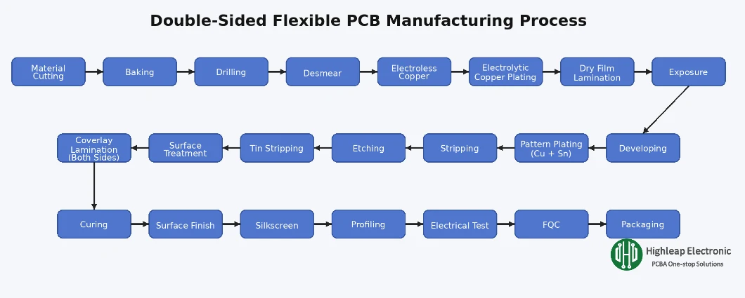
4. Double-Sided Flexible PCB Manufacturing Process
Double-sided FPC adds a second copper layer and plated through-holes (PTH) that electrically connect both sides. This increases routing density but significantly changes the process flow—drilling and plating must occur before outer layer imaging.
4.1 Complete Process Flow
Material Cutting → Baking → Drilling → Desmear → Electroless Copper → Electrolytic Copper Plating → Dry Film Lamination → Exposure → Developing → Pattern Plating (Cu + Sn) → Stripping → Etching → Tin Stripping → Surface Treatment → Coverlay Lamination (Both Sides) → Curing → Surface Finish → Silkscreen → Profiling → Electrical Test → FQC → Packaging
4.2 Key Process Differences from Single-Sided
Drilling for PTH:
Double-sided FPC requires plated through-holes to electrically connect the two copper layers. Drilling occurs through the complete FCCL stack—top copper + adhesive + PI + adhesive + bottom copper. Hole diameter is typically 0.2–0.5mm for standard applications, with microvias down to 0.1mm using laser drilling.
Desmear:
Drilling generates resin smear on hole walls that must be removed before plating. Chemical desmear (potassium permanganate) or plasma treatment etches back the resin to expose clean copper for reliable plating adhesion. This step is critical—insufficient desmear causes plating voids and poor interlayer connection.
Electroless Copper Deposition:
A thin copper seed layer (typically 0.3–0.8μm) is chemically deposited on the hole walls and surfaces through autocatalytic plating. This creates the initial conductive path for subsequent electrolytic plating. The electroless copper process includes catalyst activation (palladium-based), acceleration, and copper deposition steps.
Electrolytic Copper Plating:
Electrolytic plating builds copper thickness to design requirements—typically 20–25μm in holes for adequate reliability. Vertical continuous plating (VCP) lines provide uniform current distribution and consistent plating thickness across the panel.
Pattern Plating Process:
After copper plating, dry film is applied and imaged to expose only the circuit pattern areas. Additional copper plating builds trace thickness, followed by tin or tin-lead plating that serves as an etch resist. After stripping dry film, etching removes unwanted copper while tin protects the circuit pattern. Finally, tin is stripped to expose the finished copper traces.
Two-Sided Coverlay:
Both top and bottom surfaces require coverlay lamination to protect circuits on both sides. Registration between coverlay openings and pad locations on both sides must be carefully controlled.
5. Multilayer Flexible PCB Manufacturing Process
Multilayer FPC contains three or more conductive layers, enabling higher routing density and more complex designs. The key manufacturing difference is that inner layers must be fabricated and inspected separately before lamination—and through-hole drilling occurs after the layers are bonded together.
5.1 Complete Process Flow
Inner Layer Processing:
Material Cutting → Baking → Dry Film Lamination → Exposure → Developing → Etching → Stripping → AOI Inspection → Surface Treatment (Brown Oxide)
Lamination:
Layer Alignment → Layup → Hot Press Lamination → Post-Lamination Curing
Outer Layer Processing:
Drilling (PTH) → Desmear → Electroless Copper → Electrolytic Copper Plating → Outer Layer Imaging → Pattern Plating → Etching → Coverlay Lamination → Surface Finish → Silkscreen → Profiling → Electrical Test → FQC → Packaging
5.2 Critical Inner Layer Steps
Inner Layer Imaging and Etching:
Each inner layer is processed similarly to single-sided FPC: dry film lamination, exposure, developing, etching, and stripping. The critical difference is that inner layers must be 100% defect-free before lamination—any opens or shorts buried inside the laminated stack cannot be repaired.
AOI Inspection:
Automated Optical Inspection scans every inner layer to detect opens, shorts, trace width violations, and other defects before lamination. Defective panels are rejected at this stage to avoid wasting materials and processing time on unrecoverable boards.
Surface Treatment (Brown/Black Oxide):
Inner layer copper surfaces undergo oxide treatment to create a microscopically rough, oxidized copper surface that promotes adhesion with bondply adhesive. This step is critical—inadequate oxide treatment leads to delamination under thermal stress or during flex cycling.
5.3 Lamination Process
Layer Alignment:
Inner layers, bondply (adhesive sheets), and outer copper foils are precisely aligned using registration pins or optical alignment systems. Typical registration tolerance is ±75μm or better—misalignment causes shorts between layers or broken connections to vias.
Layup and Hot Press:
The aligned stack is placed in a lamination press and bonded under controlled temperature (typically 180–200°C peak), pressure (15–25 kg/cm²), and time profiles. The bondply adhesive flows, fills gaps, and cures to create a unified multilayer structure.
Post-Lamination Processing:
After lamination, through-holes are drilled to connect all layers. The subsequent process follows the double-sided FPC flow: desmear, electroless copper, electrolytic plating, outer layer imaging, and remaining steps through final test.
5.4 Sequential Lamination for Complex Structures
For multilayer designs requiring blind or buried vias, sequential lamination is required:
- Buried vias: Connect inner layers only—fabricated and drilled before final lamination
- Blind vias: Connect outer layer to inner layer—drilled after lamination using controlled-depth or laser drilling
Each sequential lamination cycle adds cost and lead time but enables higher density interconnects not possible with standard through-hole construction.
6. Quality Control and Industry Standards
Flexible PCB manufacturing requires systematic quality control because the thin, flexible materials are more sensitive to process variations than rigid boards. Multiple inspection gates throughout production catch defects before they become costly.
6.1 Key Inspection Points
| Process Stage | Inspection Method | Defects Detected |
|---|---|---|
| Incoming material | Visual, thickness measurement | Material defects, wrong specification |
| Post-etch (inner/outer) | AOI | Opens, shorts, trace width violations |
| Post-lamination | X-ray, cross-section (sample) | Layer misregistration, voids, delamination |
| Post-plating | Thickness measurement, cross-section | Insufficient plating, voids in holes |
| Post-coverlay | Visual, peel strength test (sample) | Misalignment, bubbles, inadequate adhesion |
| Final | Electrical test, visual inspection | Opens, shorts, cosmetic defects |
6.2 Applicable IPC Standards
- IPC-6013: Qualification and Performance Specification for Flexible/Rigid-Flex Printed Boards—defines Classes 1, 2, and 3 with increasing reliability requirements
- IPC-2223: Sectional Design Standard for Flexible Printed Boards—design guidelines including bend radius, trace routing, and material selection
- IPC-A-600: Acceptability of Printed Boards—visual inspection criteria for all PCB types including flex
- IPC-4202/4203/4204: Material specifications for flexible base materials, coverlay, and FCCL
- IPC-TM-650: Test methods for flex-specific requirements including bend testing and adhesion
6.3 IPC Class Selection
| IPC Class | Application | Typical Use |
|---|---|---|
| Class 1 | General electronic products | Consumer devices, toys, basic electronics |
| Class 2 | Dedicated service electronics | Industrial equipment, telecom, automotive |
| Class 3 | High-reliability electronics | Medical implants, aerospace, military |
7. Design Considerations for Manufacturability
Design decisions made early in the development process directly impact manufacturing yield, cost, and reliability. Following DFM guidelines helps avoid costly redesigns and production delays.
7.1 Bend Radius Guidelines
Per IPC-2223, minimum bend radius depends on application type:
- Dynamic flex (repeated bending): Minimum bend radius ≥10× total board thickness
- Static flex (bend-to-install): Minimum bend radius ≥6× total board thickness
For a 0.15mm thick single-sided FPC, this means minimum 1.5mm radius for dynamic applications or 0.9mm for static installation.
7.2 Trace Routing in Flex Areas
- Route traces perpendicular to the bend axis when possible
- Use curved traces—avoid 90° angles in flex zones
- Do not place vias, pads, or plated holes in bend areas
- Stagger traces on opposite sides of double-sided flex (I-beam effect) to reduce stress concentration
- Use hatched polygons instead of solid copper pours in flex areas to improve flexibility
7.3 Copper Weight Selection
Thinner copper improves flexibility but reduces current-carrying capacity. Balance these factors:
- 12μm (⅓ oz): Maximum flexibility, fine traces, low current
- 18μm (½ oz): Good flexibility, moderate current—most common choice
- 35μm (1 oz): Standard current capacity, reduced flexibility
- 70μm (2 oz): High current, limited flexibility—typically used only in rigid areas
7.4 Stiffener Application
Stiffeners provide mechanical support for component mounting or connector insertion in designated areas:
- FR-4: Cost-effective, common for ZIF connector areas—thickness 0.2–1.6mm
- Polyimide: Thinner profiles, better thermal match—thickness 0.075–0.225mm
- Stainless steel: EMI shielding + stiffening combined—thickness 0.1–0.3mm
- Aluminum: Heat dissipation + stiffening—thickness 0.5–2.0mm
8. Highleap’s Flexible PCB Manufacturing Services
Highleap Electronics provides complete flexible PCB manufacturing from prototype through production volume, with process control designed for consistent quality across all FPC types.
- Capability range: Single-sided, double-sided, and multilayer FPC up to 10 layers; rigid-flex construction for combined applications
- Fine-line capability: Minimum trace/space 50μm/50μm for high-density designs
- Material options: Polyimide (standard and high-performance grades), LCP for RF applications, adhesive and adhesiveless FCCL
- Surface finish options: ENIG, immersion tin, immersion silver, OSP per application requirements
- Stiffener attachment: FR-4, PI, stainless steel, aluminum with precision placement
- Assembly integration: Turnkey FPC assembly including SMT placement and functional testing
8.1 What to Include in Your RFQ
For fast, accurate quotation, provide:
- Gerber files (RS-274X format) or ODB++ data
- Fabrication drawing with dimensions, tolerances, and layer stackup
- Material specification (PI type, copper weight, adhesive/adhesiveless)
- Surface finish requirement
- Stiffener details if required (material, thickness, locations)
- Quantity (prototype and production volume estimates)
- IPC class requirement (Class 1, 2, or 3)
- Any special testing or documentation requirements
Our engineering team reviews submissions and responds with pricing, lead time, and DFM recommendations to keep your project on track.
Sabrina has over 18 years of experience in the PCB industry, with a strong background in CAM engineering and PCB file review. She supports PCB projects from prototype to volume production, focusing on manufacturability and process reliability. Her work helps engineering teams reduce production risk and achieve stable, high-quality PCB manufacturing results.

Recommended Posts
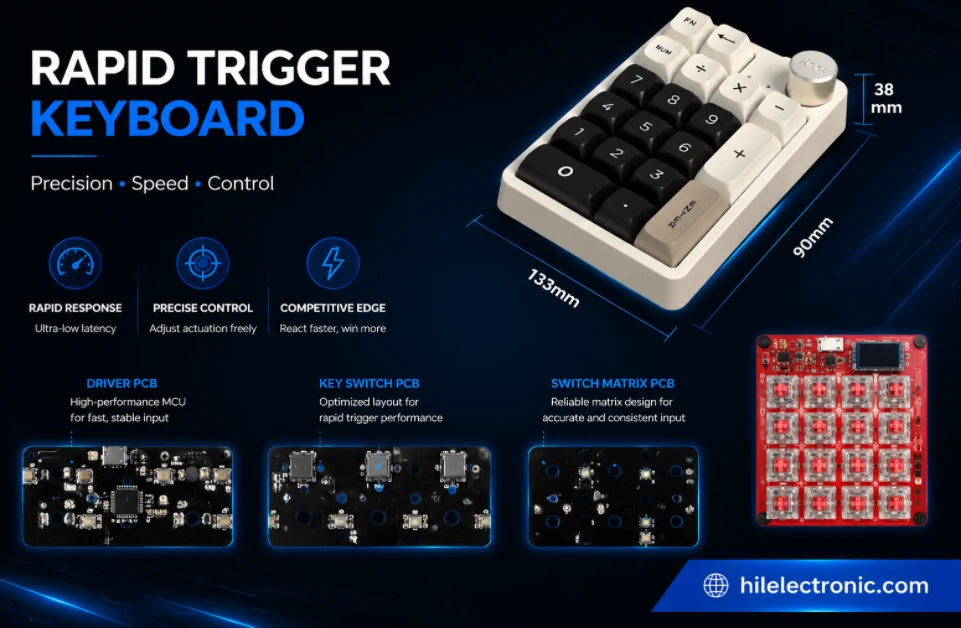
Rapid Trigger Keyboard PCB Manufacturing & PCBA
Table of contentsRapid Trigger PCBA Buying and Performance...
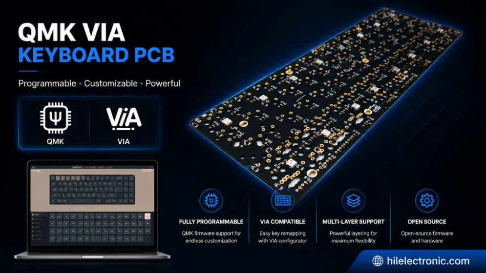
QMK/VIA Keyboard PCB Manufacturing & Assembly
Table of contentsQMK/VIA Keyboard PCB Buying...
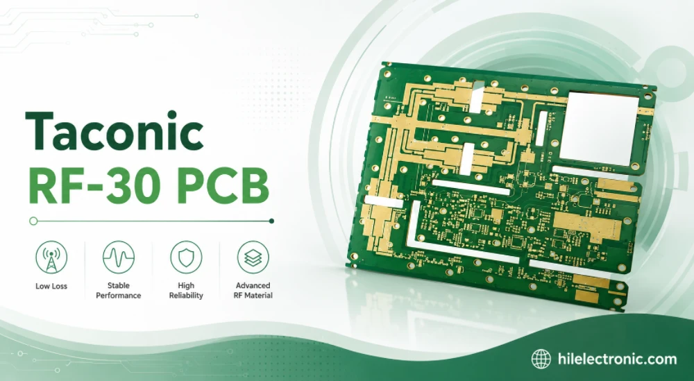
Taconic RF-30 PCB Manufacturer for Antenna and Low-PIM Boards
Table of contentsRF-30 and Current RF-30A Characteristics...
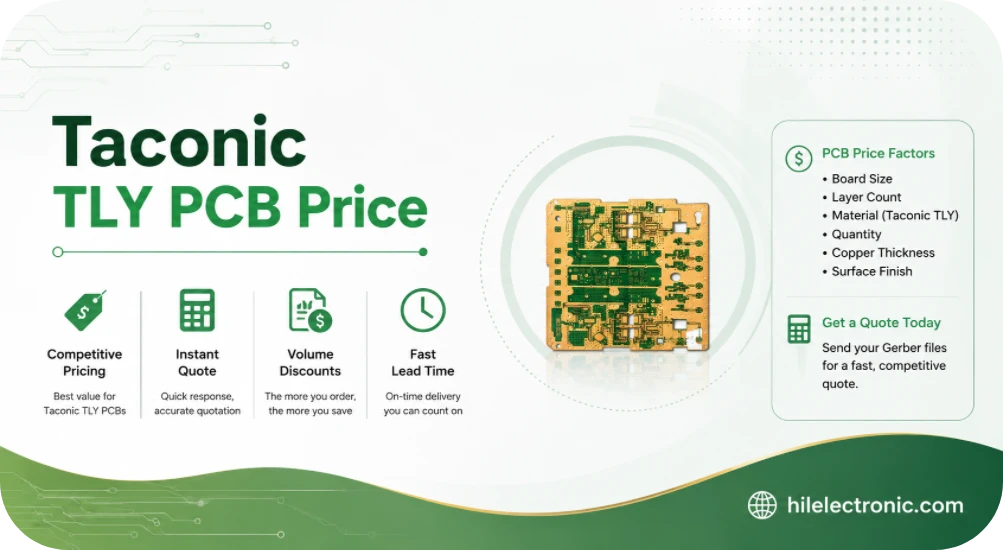
Taconic TLY PCB Price and PCBA Quotation
Table of contentsTLY-3, TLY-5 and TLY-5Z Price-Relevant...
How to get a quote for PCBs
Let us run DFM/DFA analysis for you and get back to you with a report.
You can upload your files securely through our website.
We require the following information in order to give you a quote:
-
- Gerber, ODB++, or .pcb, spec.
- BOM list if you require assembly
- Quantity
- Turn time
In addition to PCB manufacturing, we offer a comprehensive range of electronic services, including PCB design, PCBA (Printed Circuit Board Assembly), and turnkey solutions. Whether you need help with prototyping, design verification, component sourcing, or mass production, we provide end-to-end support to ensure your project’s success. For PCBA services, please provide your BOM (Bill of Materials) and any specific assembly instructions. We also offer DFM/DFA analysis to optimize your designs for manufacturability and assembly, ensuring a smooth production process.