
ITEQ IT-150G PCB Fabrication for Fine-Pitch HDI
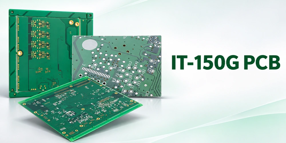
Illustration of fine-pitch multilayer PCB layouts.
ITEQ IT-150G is a halogen-free, medium-Tg epoxy system for rigid multilayer and HDI PCBs. ITEQ lists a 150°C glass transition temperature by DSC. Its suitability for a thin board depends on the depth and landing geometry of each laser microvia, which are set by the pressed stack-up and the package escape, even when the finished board thickness stays the same.
A design can pass a routing check with nominal dielectric values and still need a different build when CAM reviews the actual prepreg and copper pattern. Start the design review at the first layer transition under the component.
Start with the escape under the package
On a small controller or handheld board, a single blind via from L1 to L2 may be enough to reach a routing channel. This is a good first option in a 1+N+1 construction, where one build-up layer is added on each side of a central multilayer structure. If the next layer must remain an uninterrupted reference plane, first ask whether the net can move sideways after the first blind via and transition elsewhere. A second microvia under the first one may free routing area, but it changes the lamination sequence and introduces an additional copper interface in the vertical path.
Check the geometry that the laser will actually see
Specify the start and stop layers. Check the local cured dielectric depth, the minimum opening used in the agreed aspect ratio definition, the target pad size after etch and the remaining capture margin after layer registration. A laser via may be tapered, so the opening at the surface does not describe the contact area at the target. A shallow hole that lands partly off the target pad can still be an unreliable via. The mechanical through-hole for a connector or mounting point on the same board needs a separate drill and plating review.
Hypothetical HDI example. The same outer artwork calls for a 100 µm nominal top opening. With a 65 µm pressed build-up dielectric, the depth-to-top-opening ratio is 0.65:1. At 90 µm it becomes 0.90:1, even if a core adjustment holds the overall thickness constant. These are screening calculations. The acceptable geometry, measurement convention and registration allowance depend on the qualified process. If the revised build does not fit that process, review the dielectric and layer assignment before widening a via that shares a fine-pitch solder pad.
Record the resulting layer pairs and any buried vias in the HDI via design. Use a distinct drill definition for each span, and show whether a filled and planarized surface is part of the component land. A blind via under solder can wick solder if the specified pad treatment is missing or incomplete.
IT-150G datasheet values for the build
ITEQ identifies the copper-clad laminate as IT-150GTC and the prepreg as IT-150GBS. The core supplies a cured dielectric thickness; the prepreg bonds the layers and flows around the copper during pressing. A material callout should identify both parts of the build. IT-150GS and IT-158 are separate grade names that can appear in the same search results.
| Property | Reported result | Test basis |
|---|---|---|
| Glass transition and decomposition | Tg 150°C; Td 365°C | DSC for Tg; TGA at 5% mass loss for Td |
| Dk at 1 / 2 / 5 / 10 GHz | 3.7 / 3.6 / 3.5 / 3.5 | 75% resin content; IPC-TM-650 2.5.5.9 at 1 GHz and 2.5.5.13 at 2–10 GHz |
| Df at 1 / 2 / 5 / 10 GHz | 0.0137 / 0.0140 / 0.0145 / 0.0148 | Same resin and frequency basis as the Dk row |
| Z-axis expansion | 3.1% from 50°C to 260°C | IPC-TM-650 2.4.24; laminate specimen |
| Thermal resistance and MOT | T260 and T288 each >60 min; MOT 130°C | IPC-TM-650 2.4.24.1 for the T-times; UL 746 as listed for MOT |
Source: ITEQ IT-150G datasheet, Rev. 1.0-26. These are datasheet results on test specimens. Use the fabricator’s approved construction data to model the actual trace geometry and impedance.
This grade makes sense when the main constraint is compact interconnect and the routed channel has enough loss margin. If a long or fast lane is already close to its insertion-loss limit, compare electrical constructions before selecting IT-150G. The value at 75% resin content does not transfer automatically to a different glass style or mixed resin build.
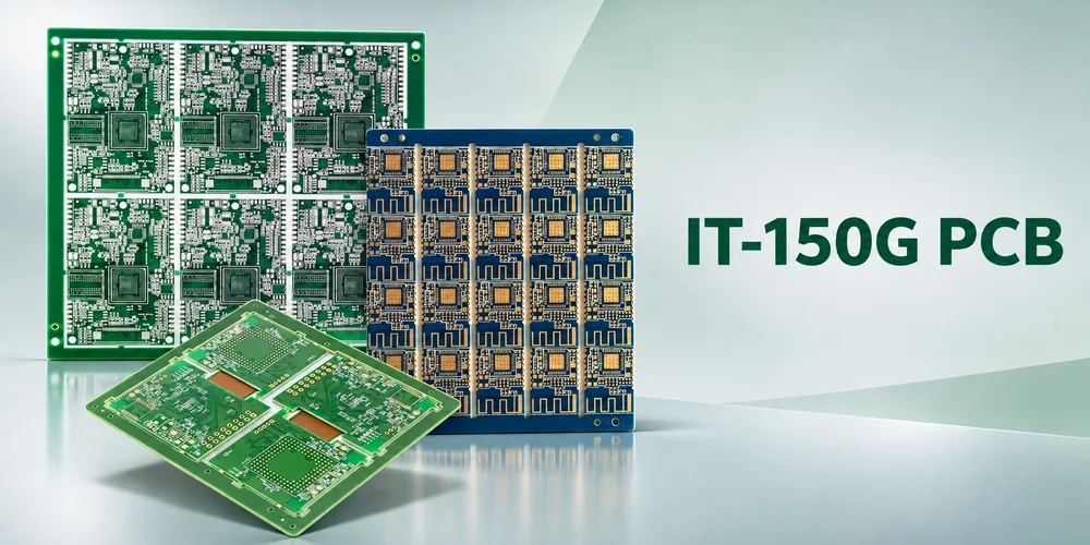
Fine-pitch PCB illustration. The released stack-up specifies the microvia geometry.
Close the resin and thickness balance before CAM release
Two areas on the same panel can demand different resin volumes. Prepreg over dense copper fills relatively little etched relief; adjacent areas cleared of copper need resin to fill the deeper recesses. If the bonding package cannot accommodate both conditions, the result can be locally thin dielectric, voids or uneven thickness. The shallow via screened earlier may then be drilled through a different dielectric depth than planned. The changes also alter the distance from a controlled trace to its reference plane.
During HDI stack-up review, compare the two build-up sides for cured thickness, copper distribution and panel support. Let CAM propose any permitted copper balancing features with keepouts for antennas, impedance references and isolation boundaries. Specify the pressed thickness as a target and tolerance with the agreed method of verification. When a glass style, prepreg construction or copper weight changes, recheck fill volume, local laser depth and impedance together. A revised materials list alone does not convey those effects to the layout or test teams.
PCB FABRICATION & ASSEMBLY
Planning an IT-150G PCB build?
Highleap can review the board construction and assembly requirements together.
Include the drill spans, target dielectric thickness and fine-pitch package land pattern.
Separate laser-via acceptance from solder-joint inspection
Microvia reliability begins at the target copper. Residue or an inadequate interface can leave a via that passes room-temperature continuity and opens when heated; a metallographic section can show capture, fill and copper geometry at the sampled plane. A thermally stressed coupon that represents the actual layer span and includes resistance monitoring can detect temperature-dependent opens that a cooled sample may conceal. Use the drawing to agree which structure represents the product and how defects will be assessed. IPC-2226A provides HDI design context; the purchase specification should separately state the applicable board acceptance and qualification requirements.
At assembly, a micro BGA adds a second problem: joint formation above the board. Verify land finish, fill and planarization, solder-mask clearance and panel support before printing paste. X-ray can examine hidden joints for issues such as solder bridging or voids, but it cannot establish adhesion at a buried microvia interface. A defect that opens during reflow needs electrical isolation to determine which interconnect failed. ITEQ’s thermal tests establish a material baseline; the assembly profile is set from the paste, components and measured temperatures of the populated board.
Release the stack-up and package together
Send the stack-up with core and prepreg designations, a drill map by layer pair and the fine-pitch land pattern. Identify fixed impedance or reference-plane requirements, which via arrangements are negotiable and what coupons or sections the acceptance plan requires. For assembly, pair those files with the BOM, placement data, finish and panel constraints. Through Highleap Electronics’ PCB and assembly quotation, the board and assembly teams can review whether the escape looks achievable with the proposed build and where a layout change may be needed before release.

About the Author
Shirley Leung
PCB/PCBA Product Manager & Technical Sales Engineer
Shirley has 5 years of hands-on experience in PCB fabrication and assembly services. Her expertise includes complex multilayer boards, HDI structures, turnkey component sourcing, SMT assembly, testing, and full system integration.
As both a technical advisor and sales specialist, she supports customers with DFM guidance, cost optimization, and production planning, helping projects move efficiently from design to mass production with consistent quality and on-time delivery.

Recommended Posts
IT-601G PCB Manufacturing for Multilayer and HDI Boards
Illustration of dense PCB routing for an HDI build.ITEQ...
FPGA Mechanical Keyboard PCB Manufacturing and Assembly
Figure 1. Assembled Clavier reference keyboard. This is an...
IT-858G Automotive PCBs for Heavy-Copper Power Control
IT-858G PCB applications in automotive electronics and...
IT-958G PCB for High Speed Servers and Backplanes
IT-958G multilayer PCB examples for server and high-speed...
How to get a quote for PCBs
Let‘s run DFM/DFA analysis for you and get back to you with a report. You can upload your files securely through our website. We require the following information in order to give you a quote:
-
- Gerber, ODB++, or .pcb, spec.
- BOM list if you require assembly
- Quantity
- Turn time
In addition to PCB manufacturing, we offer a comprehensive range of electronic services, including PCB design, PCBA, and turnkey solutions. Whether you need help with prototyping, design verification, component sourcing, or mass production, we provide end-to-end support to ensure your project’s success.
For PCBA services, please provide your BOM (Bill of Materials) and any specific assembly instructions. We also offer DFM/DFA analysis to optimize your designs for manufacturability and assembly, ensuring a smooth production process.