
Optical Transceiver PCB Cost: Compare Equivalent Quotes
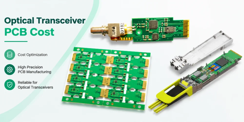
Two suppliers may quote a nominally identical six-layer optical transceiver board but include different laminates, via structures, gold-contact treatments and inspection documents. Comparing their headline unit prices without first aligning those details can lead to the wrong purchasing decision.
The central question in optical transceiver PCB cost is not “what is the cheapest price per board?” It is “what does each price actually buy?” This article works through material, fabrication, gold-finger, panel and delivery costs, then compares two hypothetical supplier offers on the same basis.
Our optical transceiver PCB service overview explains the product scope. Here the emphasis is purchasing comparison. All monetary values are teaching assumptions, not actual Highleap quotations; real prices depend on approved construction, testing, quantity and delivery.
Table of contents
OPTICAL TRANSCEIVER PCB COST
Comparing Optical Transceiver PCB Quotes?
Send the approved stackup, material, via map, contact finish, inspection scope and quantity for an itemized quotation.
Request an Optical PCB Quote →Compare the Same Approved PCB Construction
Two shops can receive the same short inquiry—“6 layers, 35 × 20 mm, optical transceiver PCB, 1,200 pcs”—and return materially different offers without either providing a like-for-like price. The missing specification may include the approved dielectric grade, channel-sensitive copper profile, blind/buried via map, hard-gold contact thickness, mechanical interface, test coupons, acceptable substitutions and delivery-unit policy. One vendor may include those items; another may assume less demanding defaults.
Before comparing amounts, identify the controlled product configuration. A proper RFQ should provide a single released revision of each fabrication file, stackup, mechanical drawing and special-process note. If the design is still evolving, mark specific items provisional and ask the supplier to quote those assumptions separately.
Six cost categories that need their own evidence
| Category | Typical source of cost difference | Information needed to compare suppliers |
|---|---|---|
| Material construction | Named low-loss cores/prepreg or hybrid laminate, copper profile and availability | Released stackup, allowed alternatives, board thickness and material notes |
| Layer/via structure | Standard through-holes vs sequential HDI, laser vias and via-in-pad filling/capping | Layer-connection drawing, drill map and via treatment |
| Contacts and mechanical fit | Selective hard gold, beveling, contact geometry, tight outlines | Contact finish map, mating interface and mechanical datums |
| Electrical and process acceptance | Continuity, impedance coupons, microsections, dimensional reports and requested insertion-loss evaluation | Actual test methods, limits, sample plan and reports |
| Quantity and arrays | NRE, panel utilization, output yield, partial arrays and shipment state | Accepted-piece quantity, panel drawing and reject policy |
| Commercial terms | Tooling, expedited material, freight, inspection exceptions and warranty/replacement terms | Explicit included/excluded items and documented delivery commitment |
A complete optical-module design may have additional priorities for 400G, 800G or 1.6T electrical channels, but the aggregate data-rate label does not establish a fixed PCB layer count or material recipe. The optical module PCB engineering article provides context for the high-speed construction requirements.
Material and Stackup: What the Quote Must Specify
A purchase request that says only “high-speed FR-4” or “low-loss PCB material” leaves substantial room for interpretation. The actual stackup determines core and bonding selections, final dielectric thickness, controlled copper weights and trace geometry. Copper surface profile and dielectric properties can matter to channel insertion loss; substitutions cannot be accepted just because two laminates have similar marketing labels.
For a fair price comparison, separate three conditions: (1) exact approved grade, (2) explicit alternate already approved by the design owner, and (3) proposed alternate awaiting qualification. Only the first two may be cost-equivalent if the approved specification actually permits both. The third is an engineering change proposal, not a valid quote for the released product.
Material procurement is also a scheduling risk. If a named prepreg or laminate is not stocked, the quote should specify material lead-time assumptions and whether the price depends on purchasing a particular panel format or minimum amount. Do not claim one brand is always more expensive; cost depends on grade, thickness, supply route and order conditions.
HDI, Drilling and Lamination Change the Process Cost
Layer count is a poor substitute for a via map. A six-layer transceiver board built with conventional plated through-holes may require fewer drilling, plating and lamination stages than another six-layer board using blind microvias, sequential lamination and filled-and-capped vias under fine-pitch packages. The latter may require additional process controls and inspection even if the final dimensions are identical.
The quote should identify which layers each blind or buried interconnect joins, whether microvias are stacked or staggered, whether via-in-pad is specified, and what filled/capped finish the customer expects. Ordinary solder-mask plugging should not be silently treated as equivalent to filled, planarized and copper-capped via-in-pad when the drawing requires the latter. The optical transceiver PCB manufacturing process explains how these operations affect the route.
Ask these three questions before accepting an HDI surcharge
- Which exact via operations are added to the production traveler, and are they present on every panel?
- What inspection and reliability requirements apply to the specified via geometry?
- Is the proposed design change approved electrically and mechanically, or is it merely a lower-cost DFM suggestion?
Do not assume that widening a line or changing a drill size is harmless. On an impedance-controlled board, those adjustments can change the electrical design and therefore need the appropriate review.
Selective Hard Gold and Mechanical Details Affect Pricing
A pluggable module may have a wear-resistant contact finish on an edge connector and a different finish on SMT pads. If the drawing states only “ENIG with gold fingers,” the supplier may not know whether selective electrolytic hard gold is actually required. The distinction influences process steps, temporary plating connections, masking, final profile and coating-thickness verification. It must be explicit in a like-for-like RFQ.
A high price is not justified merely by the word “gold”; ask what is plated, which nickel/gold specification applies, what measurements are included and how the contact edge is finished and protected. The detailed specification method is in hard gold finger PCB manufacturing.
If boards are shipped as small arrays for SMT instead of loose singles, the array can influence usable material, routing effort, rail features, depaneling risk and packaging cost. Link the delivered-unit requirement to the purchase order instead of accepting an undefined “price per set.” See PCB SET delivery and panelization for quantity arithmetic and acceptance rules.
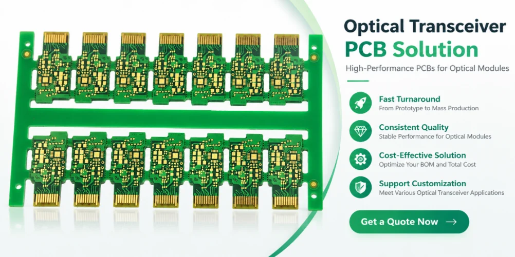
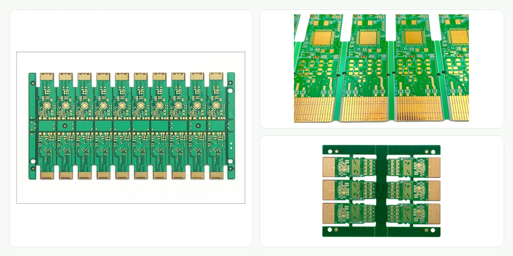
Panelized optical transceiver PCBs with gold edge contacts
Worked Comparison: Normalize Two Supplier Quotes
This entire example is hypothetical and uses invented arithmetic inputs. It is not a Highleap quotation or evidence of market prices. Imagine 1,200 accepted bare PCBs of one approved revision. The design requires a named laminate, selective hard-gold contacts, approved inspection coupons and an agreed shipment configuration.
Vendor A prices the approved construction at $9.20 per accepted board plus $600 tooling, with the specified finish, coupon reporting and delivery configuration included. Vendor B initially quotes $8.40 per board plus $250 tooling, but the fine print excludes selective hard-gold plating, the specified coupon report and array packaging. Both vendors have been asked to confirm the same laminate and HDI route before comparison.
| Bid element | Vendor A | Vendor B: initial quote | Vendor B: normalized hypothetical adders |
|---|---|---|---|
| 1,200 accepted boards | $11,040 | $10,080 | $10,080 |
| One-time tooling | $600 | $250 | $250 |
| Required selective plating | Included | Excluded | $1.35 × 1,200 = $1,620 |
| Required coupon / report scope | Included | Excluded | $420 |
| Approved array packing | Included | Excluded | $180 |
| Comparable modeled total | $11,640 | $10,330 before omissions | $12,550 |
| Modeled cost per accepted board | $9.70 | $8.61 before omissions | $10.46 |
A naïve comparison favors Vendor B at $10,330. The normalized hypothetical total becomes $12,550 versus Vendor A’s $11,640—a $910 difference in the other direction. The lesson is not that one vendor is better, nor that these adders are real market prices. It is that the commercial comparison is invalid until the product, inspection and delivery scope are the same.
A critical qualification that price normalization cannot fix
If Vendor B proposes a different laminate or unapproved via process, a buyer cannot simply add dollars to declare the offer equivalent. That offer belongs in a separate engineering-alternative column pending formal approval, possible electrical requalification and schedule assessment. A spreadsheet can normalize omissions; it cannot establish technical interchangeability.
Compare the Cost per Accepted Board
Purchasers are often offered better unit prices at larger quantities, but those tiers may use different tooling, array or production assumptions. Compare the same accepted-board quantity, drawing revision and test package at each tier. For an internal cost model, one useful decomposition is:
Total modeled order cost = nonrecurring tooling/qualification + accepted-board fabrication and inspection price × quantity + separately contracted packaging/freight and other services.
Effective cost per accepted bare PCB = total modeled order cost ÷ accepted shipped PCB quantity.
If the supplier is charging per processed fabrication panel rather than per accepted piece, you need the number of circuits per panel and a defensible expected accepted output. Do not count a rejected circuit as accepted or assume the vendor’s internal process yield is known. The volume-production panelization comparison includes a full illustrative example in which a denser panel is more costly per accepted board.
What a three-tier RFQ should actually ask
- Prototype: What minimum quantity, engineering review, tooling and inspection are included? Are any deviations from production construction being accepted for evaluation?
- Pilot/qualification: Does the build use the intended production laminate, plating, via and array route, and what first-article reports are included?
- Repeat production: What assumptions support the price tier, approved alternates, lot traceability, allowable over/under quantities and lead-time schedule?
A prototype made with a temporary alternate laminate may help debugging but should not silently become the reference cost for an approved production build. Conversely, a stable design with a fixed array and qualified process may allow setup costs to be allocated over more units. Neither rule creates a universal percentage discount.
Separate Bare PCB, PCBA and Complete-Module Scope
Quote boundaries need to be explicit. Bare-board work generally concerns the manufactured substrate, finish, electrical testing and agreed board acceptance. A PCBA quote may add purchased components, stencil and setup, SMT/THT work, AOI/X-ray and agreed board-level tests. A complete optical module can additionally require optical engines, alignment, calibration and full-system functional qualification. These are not interchangeable deliverables.
| Deliverable | Typical documentation | Do not assume it includes |
|---|---|---|
| Bare optical-transceiver PCB | PCB fabrication data, stackup, contact drawing, bare-board acceptance | BOM sourcing, component placement or finished-module optical testing |
| Populated transceiver PCBA | Above plus BOM, centroid/placement files, assembly drawings, test plan | Active optical alignment or completed optical transceiver calibration |
| Complete optical-module product | Product-level optics, enclosure, electrical and optical specifications, qualification plan | Automatically supplied by a PCB fabricator or SMT assembler |
When the buyer needs component sourcing and board population, the optical transceiver PCB assembly page should be used to define the additional scope rather than incorporating a guessed PCBA cost into a bare-board price.
A Buyer’s Quote-Comparison Checklist
For each supplier, record the approved or proposed status of every critical attribute. Use the categories below rather than relying on generic words such as “premium laminate” or “high reliability.”
| RFQ field | Minimum meaningful answer |
|---|---|
| Part number and revision | Exact released PCB and drawing revision quoted |
| Material schedule | Named core/prepreg/copper specification; listed alternatives clearly marked |
| Stackup and impedance | Approved stackup and specified coupon/measurement acceptance |
| Drills and HDI | Via map, sequential stages, fill/cap instructions and drill requirements |
| Surface finishes | Exact finish on SMT pads and on mating contacts; region map |
| Mechanical features | Finished outline, thickness, bevel/contact geometry, critical datums |
| Test and records | Electrical test, agreed coupons, microsections/measurement scope and sampling |
| Packaging and delivery | Loose or array state, good-position rule, accepted quantity, protection |
| Commercial assumptions | Setup/NRE, unit and tier price, material lead time, freight, exceptions |
| Engineering deviations | Written list of all nonconforming or proposed substitute conditions |
Red flag: A supplier refuses to specify which material grade or contact finish it priced but states that its board is “equivalent.” Equivalence should be established by the design owner against an approved requirement, not inferred from a sales description. Green flag: The quotation identifies exactly what will be fabricated and inspected, lists open engineering exceptions and gives a clear accepted-unit definition.
Common Price-Reduction Mistakes
- Replacing specified low-loss material on price alone. Savings disappear if the finished channel needs requalification or fails electrical acceptance.
- Treating all gold finishes as identical. The correct contact finish is driven by the mating requirement, while solderable pads have different needs.
- Assuming an extra board per panel is pure savings. Panel processing costs, rejected positions and downstream SMT/packing must be included.
- Ignoring test scope in quote comparisons. A basic continuity test and a specified impedance/insertion-loss program are not the same deliverable.
- Buying a larger lot just to reach a price break. Excess stock, revision changes, material age and forecast uncertainty may outweigh the nominal unit-price reduction.
Optical Transceiver PCB Cost FAQs
What is the average price of an optical transceiver PCB?
A meaningful price cannot be stated from the product label alone. Provide the actual construction, finished dimensions, layer/via structure, finishes, test requirements and accepted quantity. Public price examples with different specifications are not equivalent offers.
Are 800G or 1.6T module PCBs automatically more expensive than 400G PCBs?
Not automatically. The approved electrical lane architecture, materials, copper geometry, HDI construction, quality plan and yield determine the real processing burden. Aggregate module data rate is not a fixed fabrication recipe.
Can a supplier reduce cost by using a different laminate?
The supplier may propose an alternate, but it must be evaluated and approved where the material is part of the released electrical and reliability construction. Until then, price it as a separate proposal, not the same PCB.
Does ordering more PCB panels always lower the finished unit price?
No. The answer depends on the actual accepted-piece output, setup, defect exposure, packaging and contract. Normalize quotations to the same good-piece delivery requirement.
What should I send to get a realistic production quote?
Released Gerber/ODB++ or other agreed fabrication output, NC drill data, stackup, material and finish schedules, connector drawings, approved panel/delivery format, test criteria, accepted quantities by tier and the required delivery date. If assembly is requested, add the BOM, placement files and test plan.
Request an Itemized Optical Transceiver PCB Quote
For an optical transceiver PCB manufacturing quotation, submit the approved files and identify any pending material, via, contact-finish or delivery decisions. Ask each supplier to return pricing with a documented scope and exceptions. That gives engineering a traceable build and gives purchasing a price comparison based on the product it intends to buy.

Recommended Posts
Optical Transceiver PCB Manufacturer for Custom Pluggable Modules
Highleap Electronics manufactures and assembles custom...
Optical Module PCB Manufacturer for 400G, 800G and 1.6T Programs
Highleap Electronics provides optical module PCB...
Optical Communication PCB Manufacturer for Fiber Network Equipment
Highleap Electronics manufactures and assembles optical...
Optical Transceiver PCB Manufacturing in China
Highleap Electronics provides optical transceiver PCB...
How to get a quote for PCBs
Let‘s run DFM/DFA analysis for you and get back to you with a report. You can upload your files securely through our website. We require the following information in order to give you a quote:
-
- Gerber, ODB++, or .pcb, spec.
- BOM list if you require assembly
- Quantity
- Turn time
In addition to PCB manufacturing, we offer a comprehensive range of electronic services, including PCB design, PCBA, and turnkey solutions. Whether you need help with prototyping, design verification, component sourcing, or mass production, we provide end-to-end support to ensure your project’s success.
For PCBA services, please provide your BOM (Bill of Materials) and any specific assembly instructions. We also offer DFM/DFA analysis to optimize your designs for manufacturability and assembly, ensuring a smooth production process.