
PCB Trace Repair: Methods, Diagnosis & Best Practices

1. Introduction to PCB Trace Repair
PCB traces are thin copper pathways that establish electrical connectivity between components. When traces sustain damage from breaks, corrosion, or overheating, circuits experience open connections, impedance shifts, or intermittent failures. This guide provides systematic approaches to diagnose damaged traces and execute reliable PCB trace repair techniques.
2. Causes and Diagnosis of PCB Trace Damage
2.1 Common Causes of Trace Damage
Trace failures typically result from mechanical, chemical, or thermal factors. Mechanical stress from board flexing fractures copper at solder joints and vias. Corrosion develops from moisture ingress or battery electrolyte leakage. Excessive soldering heat or component failure vaporizes thin conductors, while undersized traces carrying overcurrent suffer electromigration damage.
2.2 How to Diagnose Damaged PCB Traces
Visual inspection under magnification reveals hairline cracks, oxidation discoloration, and burnt sections. A multimeter continuity test confirms trace integrity: open-loop readings indicate complete breaks, while abnormally high resistance suggests partial damage. Compare measurements against known-good traces to identify subtle impedance deviations.
3. Tools and Materials for PCB Trace Repair
3.1 Diagnostic and Soldering Equipment
Proper PCB trace repair requires matched tools for each repair stage:
- Digital multimeter – Enables continuity testing and resistance verification before and after repair.
- Temperature-controlled soldering iron – Fine tips (conical or chisel) provide precision for trace-level work.
- Magnification device – Loupe or stereo microscope assists damage identification and guides repair accuracy.
3.2 Repair Materials
Material selection depends on damage severity and trace application:
- 30 AWG copper wire – Standard jumper wire for bridging broken traces with minimal impedance impact.
- Conductive ink or pen – Quick application for hairline cracks in low-current signal lines.
- Copper foil tape – Replaces missing trace sections; solderable for secure termination.
- Isopropyl alcohol and flux – Surface preparation ensures proper solder wetting and adhesion.

PCB Trace Repair with Conductive Pen
4. PCB Trace Repair Methods
4.1 Conductive Ink for Minor Trace Damage
Conductive ink suits micro-fractures in low-current signal traces. Clean the damaged area with isopropyl alcohol, then apply thin layers across the break, allowing cure time between applications. This method offers quick repair without soldering but exhibits higher resistance than copper—unsuitable for power traces or impedance-controlled signals.
4.2 Jumper Wire PCB Trace Repair
The jumper wire method delivers the most reliable PCB trace repair for various damage severities:
- Expose copper – Remove solder mask on both sides of the break using a precision knife or fiberglass pen.
- Pre-tin surfaces – Apply flux and solder to exposed pads and prepared 30 AWG wire.
- Solder connections – Route wire along the shortest path; secure each end without bridging adjacent traces.
- Verify continuity – Test immediately after soldering and before applying protective coating.
4.3 Copper Tape Repair for Larger Trace Damage
Copper foil tape addresses extensive trace loss or severe corrosion. Cut tape to match original trace width and adhere along the repair path. Solder tape edges to existing trace sections for electrical continuity and mechanical stability. Conductive epoxy reinforces connections where soldering proves difficult.
When the project moves from research to an RFQ, review BOM sourcing review and fine-pitch BGA assembly so the material, process, and inspection requirements stay aligned.
5. Verification and Protection After PCB Trace Repair
5.1 Testing Repaired Traces
Continuity testing confirms basic connectivity, but comprehensive verification ensures repair quality. Measure repaired trace resistance against specifications or equivalent intact traces. Power the circuit under controlled conditions and monitor voltage levels. For RF or high-speed applications, use an oscilloscope to detect signal reflections or attenuation.
5.2 Protecting Completed Repairs
Exposed copper requires protection against environmental degradation. Apply liquid solder mask or UV-curable coating over the repaired area after testing confirms proper function. Conformal coating provides additional moisture and corrosion protection. Allow full cure time before returning the board to service.
6. When to Seek Professional PCB Trace Repair
Certain conditions exceed field repair capabilities:
- Multilayer internal breaks – Inner layer damage requires specialized equipment or board replacement.
- Controlled-impedance circuits – Standard repairs introduce parasitic effects incompatible with RF/high-speed requirements.
- Extensive corrosion or structural damage – Multiple affected traces or substrate damage warrant professional evaluation.
Recognizing these limitations ensures circuit reliability and prevents unsuccessful repair attempts.
7. Frequently Asked Questions
Can broken PCB traces be repaired at home?
Yes, most accessible single-layer and double-layer trace damage can be repaired using basic soldering equipment and jumper wire or conductive ink. Success depends on damage extent and trace accessibility.
What tools are needed for PCB trace repair?
Essential tools include a digital multimeter, temperature-controlled soldering iron, fine solder wire, flux, magnification, and repair materials such as 30 AWG wire or conductive ink.
Is conductive ink effective for high-current traces?
No. Conductive ink exhibits higher resistance than copper and suits only low-current signal traces with minimal physical stress.

Recommended Posts

RF Transceiver PCB Manufacturing and Assembly
Table of contentsRF Transceiver PCB Manufacturing and...
RFSoC Board PCB Manufacturing and Assembly One-Stop Service
Highleap Electronics supports customer-designed RFSOC...
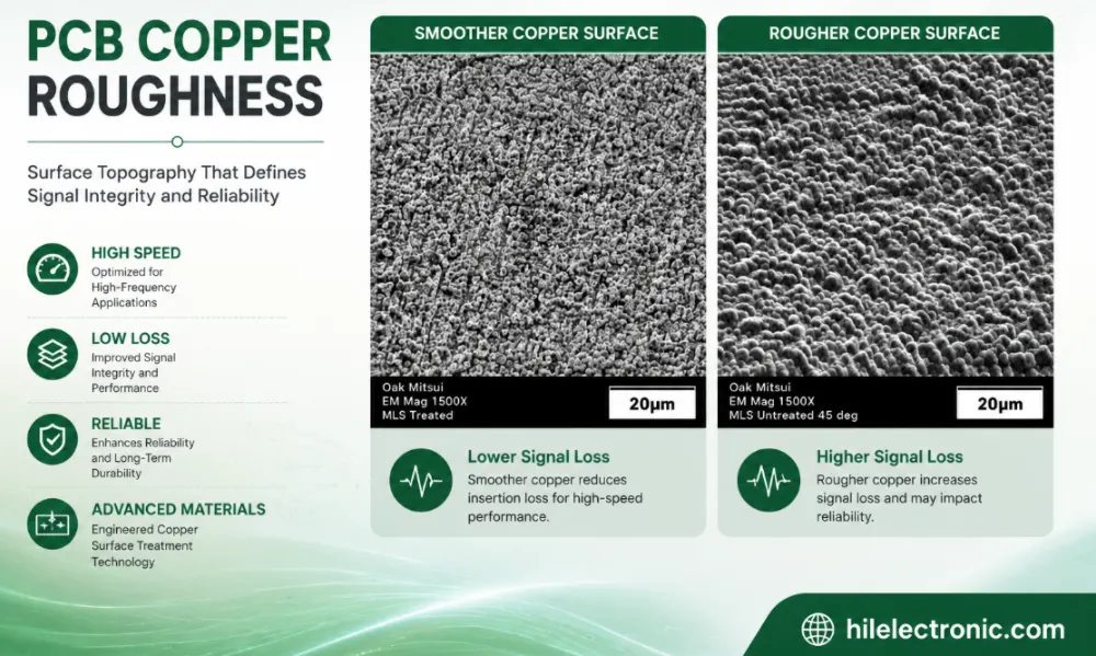
PCB Copper Roughness: Signal Loss, Material Selection and Manufacturing Control
Table of contentsWhat Is PCB Copper Roughness?How Copper...
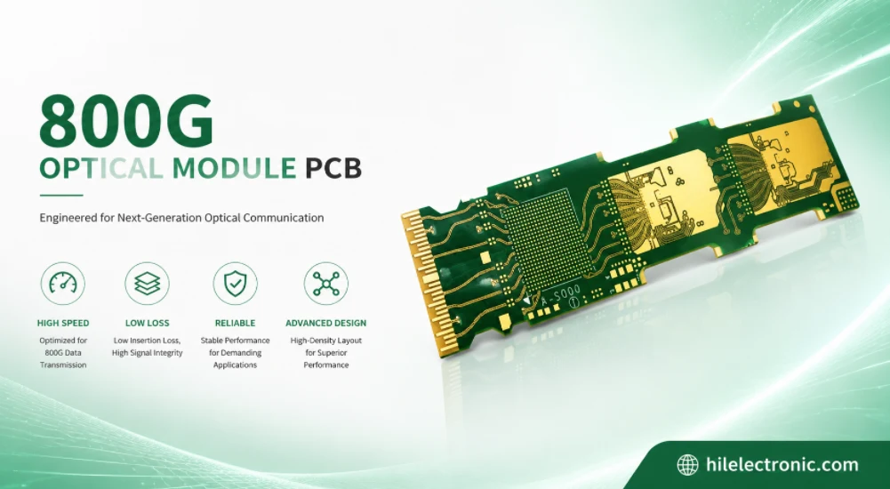
800G Optical Module PCB Manufacturing and Assembly Service
Table of contentsWhat Makes an 800G Optical Module PCB...
How to get a quote for PCBs
Let‘s run DFM/DFA analysis for you and get back to you with a report. You can upload your files securely through our website. We require the following information in order to give you a quote:
-
- Gerber, ODB++, or .pcb, spec.
- BOM list if you require assembly
- Quantity
- Turn time
In addition to PCB manufacturing, we offer a comprehensive range of electronic services, including PCB design, PCBA, and turnkey solutions. Whether you need help with prototyping, design verification, component sourcing, or mass production, we provide end-to-end support to ensure your project’s success.
For PCBA services, please provide your BOM (Bill of Materials) and any specific assembly instructions. We also offer DFM/DFA analysis to optimize your designs for manufacturability and assembly, ensuring a smooth production process.