
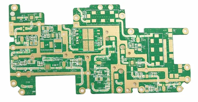
Taconic RF-60A Antenna PCB Supplier | Turnkey Assembly

When engineering microwave filters, power amplifiers, and phased array antenna feed networks, hardware teams face a strict signal integrity budget. Conventional FR-4 laminates introduce unacceptable insertion loss and phase shifting at elevated frequencies. To maintain signal clarity, engineers specify PTFE-based substrates like Taconic RF-60A. With a dielectric constant of 6.15, it offers an optimal balance between circuit miniaturization and low-loss electrical performance.
However, selecting the right material is only the first step. The true field performance of your board depends entirely on the factory’s ability to control trace geometry, drilling quality, and plating reliability on a chemically inert Teflon substrate. Finding a capable China Taconic RF-60A PCB manufacturer means partnering with a specialized PTFE PCB fabrication facility that protects your RF design tolerances from the initial layout through mass production. At Highleap Electronics, we bridge the gap between electrical simulation and physical manufacturability.
Submit Your RF-60A Project for a DFM Review
Comprehensive DFM Table of Contents
Technical Specs of the RF-60A Microwave Printed Circuit Board
An RF-60A microwave printed circuit board is built on a woven glass-reinforced PTFE composite designed specifically for high-performance RF applications. When engineers select this material from our advanced microwave dielectric materials portfolio, they rely on specific datasheet metrics to ensure phase stability and thermal reliability.
- Dielectric Constant (Dk): 6.15 ± 0.15 (at 10 GHz). This elevated Dk allows for significant circuit miniaturization compared to standard Dk 3.5 materials, making it ideal for compact RF modules.
- Dissipation Factor (Df): 0.0028 (at 10 GHz). Ensures ultra-low insertion loss for passive microwave components and feed networks.
- Thermal Conductivity: 0.41 W/mK. Optimized to handle the heat dissipation requirements of surface-mounted RF power amplifiers used in complex telecom board assemblies.
- Moisture Absorption: 0.02%. Water has a highly disruptive dielectric constant. This low absorption rate guarantees stable impedance performance even in exposed outdoor antenna enclosures.
Bottlenecks in RF-60A Low Loss Board Fabrication
Producing a custom Taconic RF-60A high frequency PCB is fundamentally different from manufacturing standard rigid FR-4. The material’s woven glass PTFE composition aggressively resists standard chemical processing. To guarantee that your physical board matches your HFSS or CST simulations, a competent factory must master three critical fabrication stages.
1. Trace Etching and LDI Precision
Because the Dk of RF-60A is 6.15, your 50-ohm RF traces will be considerably narrower than those on a lower-Dk substrate. A standard chemical etching bath will easily over-etch these microscopic lines, eating into the sidewalls of the copper. This creates a trapezoidal trace profile that shifts the characteristic impedance and causes severe signal reflection.
To prevent this during RF-60A low loss board fabrication, Highleap exclusively utilizes Laser Direct Imaging (LDI) rather than traditional film masks during our millimeter-wave PCB processing. LDI ensures perfectly vertical trace sidewalls with a tolerance of ±10%. Furthermore, we strongly advise designers to specify 0.5 oz (18 μm) or 1 oz (35 μm) base copper. Heavy copper (2 oz or more) inherently requires prolonged chemical etching that unavoidably undercuts narrow microwave traces.
2. PTFE Metallization and Plasma Desmear
Teflon is chemically inert and naturally hydrophobic (water-repelling). If a factory drills an RF-60A board and runs it through a standard electroless copper plating line, the liquid copper will bead up and peel right off the smooth via walls. This leads to fatal open circuits when the board undergoes thermal shock during SMT reflow.
Successful Taconic RF-60A circuit board making requires strict fluoropolymer activation. Before plating, we place the drilled panels into a vacuum plasma chamber, ionizing a precise mixture of CF4 and Oxygen gases. This high-energy plasma physically bombards the PTFE, micro-roughening the hole wall to create a hydrophilic surface. This guarantees that the palladium catalyst and subsequent copper plating anchor securely to the via barrel, achieving IPC Class 3 manufacturing standards.
3. Dimensional Scaling for Multilayer Registration
Despite the woven fiberglass reinforcement, the PTFE polymer retains massive internal mechanical stresses from its lamination process at the raw material plant. During high-density multilayer bare board production, when we etch away heavy copper ground planes to form your circuitry, these built-in stresses are violently released, causing the material to shrink anisotropically.
When aligning ultra-fine RF traces across 8 or 10 layers, uncompensated shrinkage causes via breakouts and disastrous layer misregistration. Our CAM engineers resolve this by running first-article test panels to calculate exact X/Y dimensional scaling factors. These compensation ratios are applied directly to your Gerber artwork before LDI exposure, ensuring perfect layer-to-layer alignment.
Hybrid Stackups: Lowering Your Taconic RF-60A PCB Fabrication Quote
High-frequency PTFE laminates represent a significant portion of your BOM cost. Using RF-60A for every single layer of an 8-layer board is a massive waste of your procurement budget if only the top layer carries the microwave signal.
To calculate your hybrid RF stackup pricing and significantly lower your Taconic RF-60A PCB fabrication quote, we specialize in asymmetric hybrid stackup engineering. We utilize the expensive RF-60A material exclusively for the critical outer layers, and bond it with cost-effective, high-Tg FR-4 for your internal digital logic and power planes. By applying customized, slow-ramp thermal press recipes, we fuse these dissimilar materials perfectly without inducing asymmetric warpage.
DFM Guideline: Prepreg Selection for Hybrid Builds
When designing an RF-60A hybrid stackup, do not specify PTFE bonding films to bond the FR-4 to the RF-60A core. The lamination melt temperatures of PTFE and FR-4 are fundamentally incompatible. Specify high-Tg epoxy prepregs or specialized low-loss thermoset prepregs to ensure a reliable and flat lamination press cycle.
Lead Times for a Taconic RF-60A Microwave PCB Prototype
Time-to-market is critical in the telecommunications sector. Waiting weeks for a factory to source raw materials from overseas brokers is unacceptable. We maintain a strategic inventory of popular high-frequency PTFE laminates, allowing us to launch your Taconic RF-60A microwave PCB prototype immediately after DFM approval.
We do not leave your RF performance to chance. We cross-reference your trace widths against our exact factory etching factors using specialized microwave etching protocols and Polar Instruments impedance calculators. Following production, we test the physical impedance coupons using Time Domain Reflectometry (TDR) equipment. Every production batch is shipped with a comprehensive TDR test report, providing documented proof that your high-Dk boards meet your exact 50-ohm specifications.
Turnkey Assembly from a Taconic RF-60A RF PCB Factory
Moving sensitive PTFE boards from a bare board fabricator to a separate assembly house introduces severe logistical risks. Handling scratches across a critical microscopic RF trace can easily alter the impedance, destroying the module’s tuned performance.
To eliminate supplier finger-pointing, Highleap Electronics operates as a comprehensive Taconic RF-60A RF PCB factory and a dedicated Taconic RF-60A antenna PCB supplier. We seamlessly transition your project from our bare board wet processing lines directly into our turnkey surface mount technology (SMT) lines.
By keeping your project entirely under one roof, we develop customized thermal reflow profiles that respect the PTFE substrate and utilize 3D X-Ray (AXI) inspection to guarantee void-free thermal grounding beneath high-power RF components. Contact our engineering team today to submit your Gerber files and BOM.

Recommended Posts
Rogers TMM6 PCB Manufacturing for Microwave Filters
Table of contentsWhy Microwave Filter Designers Use...
Taconic fastRise 27 Prepreg PCB Bonding and HDI Fabrication Service
Table of contentsWhat fastRise 27 Is—and What You Are...
Rogers RT/duroid 6010.2LM PCB Manufacturer and Fabrication Service
Table of contentsIs RT/duroid 6010.2LM the Right Material...
Panasonic R-5785(N) MEGTRON 7 PCB Manufacturer and Fabrication
Table of contentsWhen a Design Should Move to R-5785(N) /...
How to get a quote for PCBs
Let us run DFM/DFA analysis for you and get back to you with a report.
You can upload your files securely through our website.
We require the following information in order to give you a quote:
-
- Gerber, ODB++, or .pcb, spec.
- BOM list if you require assembly
- Quantity
- Turn time