
HDI PCB Guidelines for Server Motherboards

HDI Adoption Criteria for Server Motherboards
Build Server Motherboards: HDI stackup examples, microvia/VIPPO rules, materials, impedance sign-off, and DFM tips to cut cost and lead time. Server baseboards and AI accelerator boards push density, bandwidth, and power far beyond standard designs. HDI is justified when:
- Fine-pitch packages dominate (CPU sockets, chipsets, BMC, retimers; BGAs at ≤ 0.5 mm, down to 0.3–0.4 mm with VIPPO).
- High-speed fabrics (PCIe Gen5/6, CXL, NVLink/PCIe retimers) require short vertical transitions and minimal stubs.
- Memory topologies (DDR5 RDIMM/LRDIMM, HBM mezzanines/modules) need tightly controlled impedance and skew.
- I/O escape pressure around CPU/GPU footprints would otherwise explode layer count or force heavy back-drilling.
- Mechanical constraints (EEB/CEB/server card outlines, keep-outs, heat sinks, stiffeners) limit routing channels.
From HDI Adoption Criteria to Stackup Choices for Server Motherboards
You’ve defined why HDI is needed. This section turns those criteria into how to configure the stackup so routing density, SI/PI, reliability, and assembly align.
Design inputs → What they drive in the stackup
- BGA pitch & I/O density → HDI order (outer µvia layers first), staggered vs. stacked strategy, VIPPO scope, annular-ring targets, and lamination-cycle count.
- High-speed fabrics (PCIe Gen5/6, CXL, retimers) → outer-layer µvia transitions to minimize stubs, dielectric loss class selection, tight plane adjacency, and any controlled back-drill residuals.
- Memory topology (DDR5 RDIMM/LRDIMM, HBM modules) → spread-glass choices, dielectric step options, skew control, and coupon strategy by topology.
- Power & thermals → copper-weight zoning, via farms/thermal-via arrays, symmetric copper to contain panel warp, bow/twist targets.
- Mechanical envelope (EEB/CEB, heatsinks, stiffeners) → routing-channel availability, layer budgeting, keep-out-driven via planning.
- Assembly & test → VIPPO planarity, stencil rules for 01005/0.3 mm pitch, X-ray windows, ICT/boundary-scan access.
Practical selection flow
- Fix BGA pitches and escape patterns around CPU/GPU/ASIC footprints.
- Choose the lowest HDI order that cleanly escapes using staggered µvias wherever possible.
- Lock a single dielectric family per panel and your impedance targets; back-solve widths/spaces with outer-layer plating allowance.
- Balance copper and confirm lamination cycles; add stacked µvias only when routing proves it’s required.
- Define VIPPO fill/planarity specs; place impedance coupons and X-ray sample regions.
- Run FA with impedance + micro-sections; make minor dielectric tweaks, then freeze the mass-production stackup.
Typical outcomes for Server Motherboards
- Mainstream rack baseboard: low-to-mid HDI order; outer-layer µvias, limited buried structures; minimal lam cycles. These designs often form the foundation for server motherboard PCB assembly projects.
- Dense GPU/accelerator carrier: VIPPO under fine-pitch BGAs, selective buried vias; mid HDI order with careful copper balance. Such layouts are increasingly relevant for AI motherboards, where high-speed fabrics and tight routing dominate.
- OAM/SXM-class boards: extreme I/O density; higher HDI order, strict planarity and process controls, non-linear cost sensitivity. These cutting-edge configurations align with AI computing hardware PCB manufacturing requirements.
HDI PCB Stackup Examples for Server Motherboards
The diagrams below are simplified examples of first- to eighth-order HDI architectures. They show via types, lamination sequences, and layer ordering only; they are not final or buildable stackup selections. For a program-specific stackup recommendation, share your target impedances, material family, copper weights, layer count, and surface finish. Our engineering team will return a manufacturable proposal with coupon design, tolerances, and DFM notes.
• Surface blind vias
• Minimum via size: 0.1mm
• 4-layer stackup
• Stacked blind vias
• Minimum via size: 0.08mm
• 6-layer stackup
• Buried via technology
• Minimum via size: 0.075mm
• 8-layer stackup
• Complex buried structure
• Minimum via size: 0.065mm
• 10-layer advanced design
• Multi-layer buried structure
• Minimum via size: 0.05mm
• 12-layer AI-optimized design
• Ultra-high density interconnect
• Minimum via size: 0.04mm
• 14-layer supercomputing design
• Extremely high density design
• Minimum via size: 0.03mm
• 16-layer cutting-edge design
• Maximum density interconnect
• Minimum via size: 0.025mm
• 18-layer ultimate design
HDI DFM Guidelines for Server Motherboards: From Examples to Production
With the HDI PCB Stackup Examples for Server Motherboards in mind, the next step is converting those visuals into a buildable stack that meets cost, yield, and lead-time targets. Use the following DFM rules to stay inside a stable manufacturing window.
Routing and Feature Sizes
- Trace/space (outer/inner): 75/75 µm is typical. If you target 60/60 µm, confirm copper thickness and impedance so plating margins do not shift SI.
- Laser microvias: 75–100 µm diameter, aspect ratio ≤ 1:1, annular ring ≥ 50–60 µm for reliability and plating yield.
- Staggered vs. stacked: Prefer staggered microvias; if stacking is unavoidable, limit to ≤ 2 stacked pairs per side.
- Blind/buried mix: Minimize lamination count; a 1+N+1 structure often outperforms 2+N+2 for server motherboards on cost and schedule.
- Drill-to-copper (inner layers): ≥ 200 µm to reduce CAF risk and sensitivity to drill wander.
VIPPO, Solder Mask, and Panelization
- VIPPO (via-in-pad, plated over): Specify IPC-4761 Type VII, fill material, minimum fill %, and over-plate thickness. Define a planarity target up front.
- Fine-pitch BGA mask: For non-VIPPO escapes, keep mask dam ≥ 80–100 µm to prevent solder wicking.
- Copper balance: Maintain symmetry and add thieving where local coverage > 60% to control warpage on large baseboards.
- Panelization: Use 18″×24″ or 21″×24″ and keep a single resin family per panel to stabilize impedance and yield.
Primary Cost and Lead-Time Levers
- Lamination cycles: biggest driver—select the lowest HDI order that cleanly escapes your BGAs.
- Microvia count and stack height: favor staggered to protect plating yield and cycle time.
- Material systems: one resin family per panel lowers variability and simplifies qualification.
- Surface finish: ENIG / ENEPIG / OSP—choose for assembly flow and reflow count.
- Tolerances: tight impedance, thickness, and warp specs increase process time and cost—hold them only where they matter.
How Highleap Electronics Helps Server Motherboard Teams
- Stackup co-design: translate your example stackup into a manufacturable build with confirmed materials, dielectric steps, and plating allowances.
- Impedance sign-off: provide coupon design and acceptance bands; run FA with impedance and micro-sections before mass production.
- VIPPO and via quality: define fill/planarity specs, X-ray sampling, and void criteria to protect BGA yield.
- Risk-based DFM: deliver a ranked list (SI/PI, warpage, drill-to-copper, panel strategy) with practical mitigations.
- Build options: prototype, pilot, and volume HDI PCB + turnkey PCBA for server motherboards and related cards (OCP NIC, PCIe risers, NVMe backplanes).
Ready to review your design? Share your target impedances, material preferences, and manufacturing data (Gerber/ODB++/IPC-2581). We’ll return a stackup proposal, DFM notes, and clear trade-offs—engineer-first, production-ready.

Material Selection and Impedance Control for Server Motherboard HDI PCBs
Choose dielectric systems for the target data rate and thermal profile, then lock impedance with coupons before first articles.
Material Strategy
- Data rates: 10–28 Gbps NRZ can fit low-loss FR-4+; ≥ 28 Gbps or PAM4 typically requires mid/low-loss resin systems.
- Glass and resin: Model Dk/Df, glass style, resin content, and copper roughness; consider spread glass or route-on-bias to mitigate weave-induced skew on DDR5.
- Thermal robustness: Use high-Tg (≥ 170 °C), low-CTE dielectrics for multi-reflow and thermal shock common in server motherboard assembly.
- Compliance and reliability: If halogen-free, tin-whisker, or CAF limits are required, state test methods and thresholds in the specs.
Impedance Sign-Off Flow
- Provide a target impedance table (e.g., 50 Ω SE / 100 Ω Diff, ±10%) with intended reference-plane topology per layer.
- Receive candidate stackups with back-solved widths/spaces and outer-layer plating allowances.
- Jointly freeze finished copper thickness, dielectric tolerances, coupon design/placement, and acceptance bands.
- Run first-article impedance and micro-section; make minor adjustments if needed, then lock the mass-production stackup.
Copy-Ready Notes for Server Motherboards
Controlled Impedance: 50 Ω SE / 100 Ω Diff (±10%). Use supplier-confirmed stackup and standard coupons; outer-layer widths include plating allowance.
Material: Single low-loss family across all dielectrics; consistent glass style and resin content to maintain stable Dk/Df. Cross-family mixing not permitted.
Microvias, VIPPO, and Assembly Co-Design for Server Motherboards
Reliability on server motherboards depends on via structure, fill/planarity, and the reflow profile—treat them as one closed loop.
Via Quality and Planarity
- Via fill quality: Define fill type, minimum fill %, and planarization/over-plate (e.g., ≥ 20 µm) in fab notes.
- VIPPO planarity: Drives BGA wetting and voiding; include X-ray sampling and void assessment in FA (target < 10–15%).
- Known failure modes: Microvia knee cracking, resin recession, and electro-migration at transitions; validate with multi-reflow (e.g., 6× @ 260 °C) and IST/thermal shock as required.
Assembly Collaboration Checklist
- Reflow profile: Align to Tg/CTE and VIPPO chemistry; avoid excessive peak temp/TAL that increases metal-resin stress.
- BGA escapes: Prefer VIPPO; otherwise manage solder-mask dams/windows to prevent wicking on fine pitch.
- Warp control: Symmetric stack, copper balance, and proper tooling/support; set panel warp spec (e.g., ≤ 0.7%).
- Fine-feature readiness: For 01005 or 0.3 mm-pitch BGAs, coordinate stencil apertures, tolerances, and any local step-downs/ups.
- Surface finish: ENIG for general fine pitch; ENEPIG for mixed soldering/wire-bond; OSP is economical but reflow-count sensitive; ImmAg/ImmSn need storage and sulfur/tin-whisker controls.
Server Motherboard RFQ Package Checklist
- Gerber / ODB++ / IPC-2581 (prefer ODB++ or IPC-2581)
- Stackup table (brand/model, dielectric thicknesses, copper weights)
- Impedance targets and coupon requirements
- Drill chart (laser/mechanical, VIPPO, back-drill, buried)
- Finish, solder mask/legend, flammability rating
- Panelization and depanel rules (V-cut/tab-route), critical outline tolerances
- For PCBA: BOM, centroid (XYRS), stencil guidance, target reflow profile
Ready to build? Share your target stackup, impedance goals, and manufacturing data. Highleap Electronics will return a manufacturable proposal, a ranked DFM/SI/PI risk list, and clear options on finishes, lamination cycles, and materials—engineer-first, production-ready.

What We Do for Server Motherboards
1) Architecture & Stackup Co-Design
- HDI stackups from 1st to 8th order matched to BGA pitch, routing density, and budget.
- Impedance planning for PCIe Gen5/6, CXL, DDR5, and retimer chains, including plane strategy and return-path continuity.
- Coupon design and placement for controlled-impedance sign-off; guidance on glass-weave mitigation and copper balance.
- Back-drill vs. HDI trade-off analysis to minimize stubs and lamination cycles.
2) DFM Review with Ranked Risk Register
- Line/space, microvia aspect ratio, stacked vs. staggered strategy, VIPPO requirements, drill-to-copper, and mask rules near fine-pitch BGAs.
- A severity-ranked list (impact, root cause, fix) so your layout team knows exactly what to change and why—before prototypes.
3) Material & Finish Strategy
- Selection across low-loss to ultra-low-loss resin systems based on data-rate, thermal profile, and supply risk.
- Single resin family per panel where possible to stabilize impedance and yield.
- Finish trade-offs (ENIG / ENEPIG / OSP / ImmAg / ImmSn) aligned to assembly flow and reflow count.
4) NPI, FA, and Pilot Builds
- First articles with impedance measurements and micro-sections; X-ray sampling of VIPPO and fine-pitch BGA regions.
- DOE options for via-fill/planarity, warpage control, and stencil/reflow parameters on 01005 / 0.3 mm pitch.
- Reliability checks coordinated as needed (e.g., thermal cycling, IST) with clear acceptance criteria.
5) Turnkey PCBA for Server Programs
- Stencil design (apertures, step-ups/downs), reflow profiling matched to Tg/CTE and VIPPO chemistry.
- SPI, AOI, X-ray, flying-probe/ICT where applicable; boundary-scan/JTAG chain integration and basic functional harness collaboration.
- Rework capability on fine-pitch BGAs and large CPUs/ASICs; serialisation/traceability and lot-level documentation.
6) Related Boards in the Same Program
- Backplanes (NVMe/SAS/SATA), PCIe risers/retimer cards, OCP NIC/mezz cards, power distribution boards, fan-controller and management boards, front-panel I/O PCBs. These are often part of larger server PCB manufacturing programs.
- Where feasible, align stackups/material families across these boards to simplify impedance control, coupons, sourcing, and qualification.
7) Supply Chain & Lifecycle Support
- BOM feasibility and alternates, AVL alignment, LTB/EOL risk calls, and second-source proposals.
- Lot-level documentation packs (material data, test results, travelers) and FA support for any field returns.
8) Build to Your Acceptance Criteria
- We manufacture to customer-specified standards and acceptance criteria (e.g., IPC-A-600/610 Class 2/3 when specified), with measurement data attached to first articles. For performance-driven applications, this approach aligns closely with high-performance computing PCB manufacturing and GPU PCB manufacturing.

Related Articles
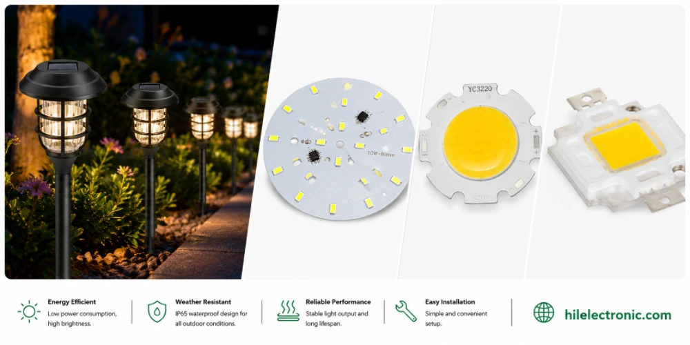
LED Garden Light PCB Manufacturing & Assembly by Highleap Electronics
Figure 1. LED garden light PCB production and assembly...
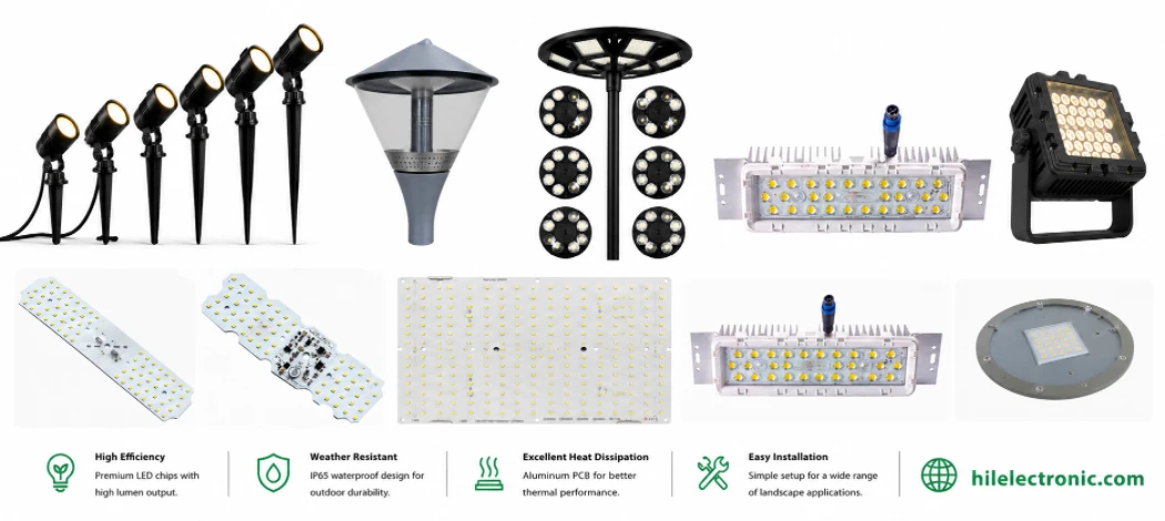
LED Landscape Light PCB Manufacturing — Uplight, Well Light & Underwater Engines
Figure 1. LED landscape light PCB production and assembly...
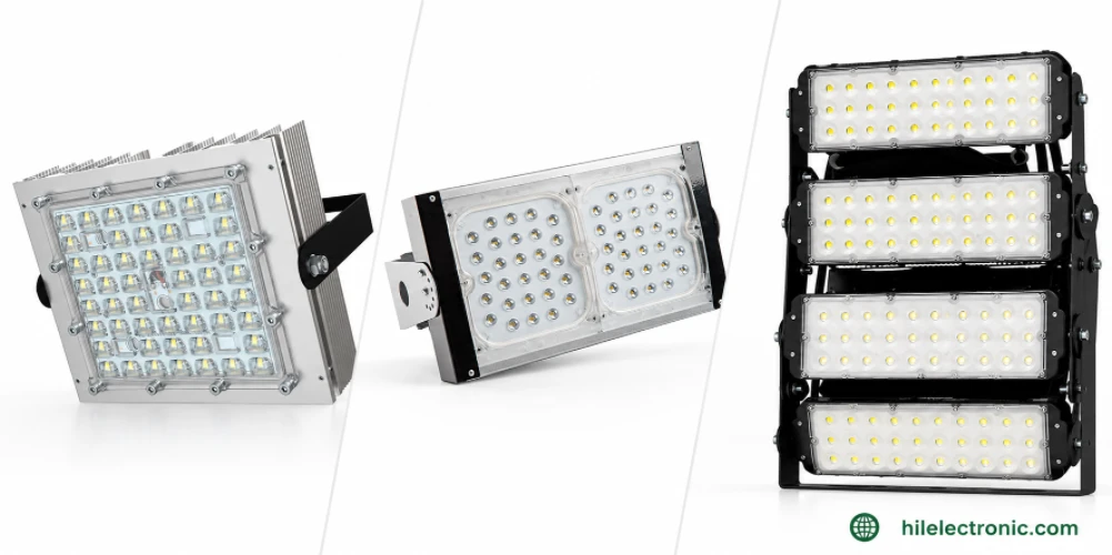
LED Parking Lot Light PCB Manufacturing & Assembly by Highleap Electronics
Figure 1. LED parking lot light PCB production and...
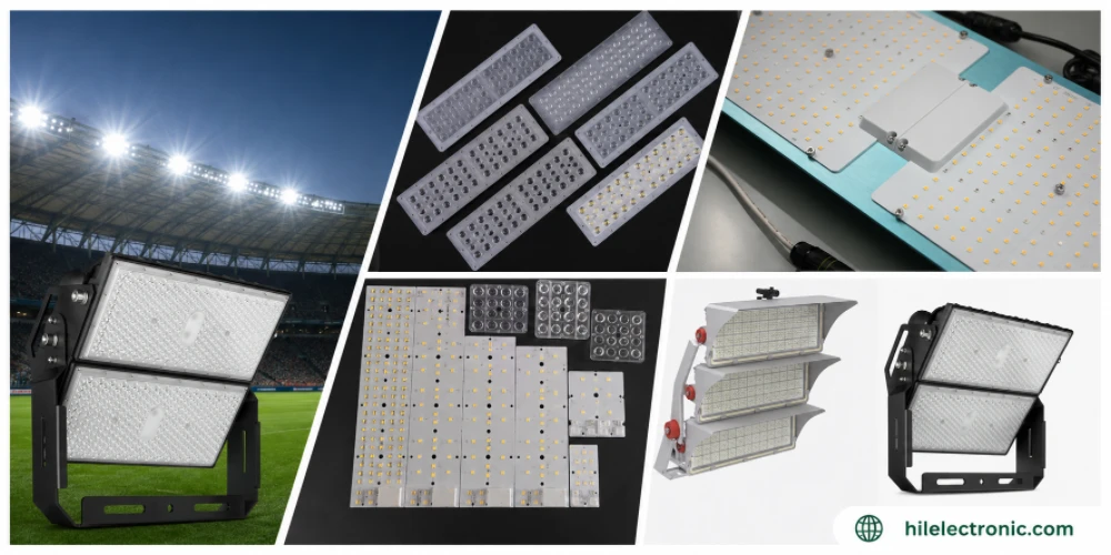
LED Stadium Light PCB Manufacturing — Very-High-Power Engines & Flicker-Free Drivers
Figure 1. LED stadium light PCB production and assembly...
How to get a quote for PCBs
Let us run DFM/DFA analysis for you and get back to you with a report.
You can upload your files securely through our website.
We require the following information in order to give you a quote:
-
- Gerber, ODB++, or .pcb, spec.
- BOM list if you require assembly
- Quantity
- Turn time
In addition to PCB manufacturing, we offer a comprehensive range of electronic services, including PCB design, PCBA (Printed Circuit Board Assembly), and turnkey solutions. Whether you need help with prototyping, design verification, component sourcing, or mass production, we provide end-to-end support to ensure your project’s success. For PCBA services, please provide your BOM (Bill of Materials) and any specific assembly instructions. We also offer DFM/DFA analysis to optimize your designs for manufacturability and assembly, ensuring a smooth production process.