
Professional AI Motherboard PCB Manufacturing Solutions

AI Motherboard Architecture and Technical Requirements
AI motherboard PCB manufacturing demands premium materials and specialized processes to achieve the performance and reliability required for mission-critical AI applications.
AI motherboard PCBs differ significantly from conventional computer motherboards due to their specialized requirements for handling artificial intelligence workloads. These boards must support multiple high-performance processors, specialized AI accelerator chips, extensive memory arrays, and sophisticated power management circuits.
Key technical specifications for AI motherboard PCBs include:
- Layer Count: Typically 12-32 layers to accommodate complex routing requirements
- Signal Speed: Support for PCIe 5.0/6.0 standards with data rates exceeding 32 GT/s
- Power Delivery: Multi-phase voltage regulators capable of delivering 200-500W per processor
- Memory Support: High-speed DDR5, HBM3, and specialized AI memory interfaces
- Thermal Considerations: Advanced copper pour strategies and thermal via arrays
- Form Factors: Custom designs optimized for rack-mount servers and blade systems
- Connector Density: High-density interconnects for accelerator cards and expansion modules
The architectural complexity requires careful signal integrity analysis, power integrity simulation, and thermal modeling during the design phase to ensure reliable operation under demanding AI computational loads.
Advanced Materials and Manufacturing Processes
AI motherboard PCB manufacturing demands premium materials and specialized processes to achieve the performance and reliability required for mission-critical AI applications.
| Material Property | Standard PCB | AI Motherboard PCB | Server Grade PCB |
|---|---|---|---|
| Dielectric Constant (Dk) | 4.2-4.5 | 3.3-4.0 | 3.5-4.2 |
| Dissipation Factor (Df) | 0.020-0.025 | 0.008-0.015 | 0.012-0.020 |
| Thermal Conductivity | 0.3 W/mK | 0.8-1.2 W/mK | 0.6-1.0 W/mK |
| Copper Weight | 1-2 oz | 2-4 oz | 2-3 oz |
| Via Fill | Optional | Required | Recommended |
Material Selection Considerations:
- Low-Loss Dielectrics: Rogers RO4000 series, Taconic TLY, or Isola I-Speed materials for high-frequency performance
- Thermal Interface Materials: Specialized prepregs with enhanced thermal conductivity for heat dissipation
- Copper Foil: High-frequency optimized copper with controlled surface roughness
- Solder Mask: High-temperature resistant materials suitable for reflow temperatures above 260°C
- Surface Finishes: ENIG, OSP, or hard gold depending on connector and component requirements
The manufacturing process involves precision drilling for microvias, controlled impedance routing, and multiple lamination cycles to achieve the required layer count and performance characteristics.
Design Guidelines and Signal Integrity Optimization
Successful AI motherboard PCB design requires adherence to strict guidelines that ensure signal integrity, power integrity, and electromagnetic compatibility under high-speed operation. These practices are especially critical in complex applications such as server motherboard PCB assembly, AI computing hardware PCB manufacturing, and large-scale server PCB manufacturing.
Critical Design Rules:
- High-Speed Signal Routing: Maintain controlled impedance (typically 50Ω single-ended, 100Ω differential)
- Length Matching: Strict timing requirements for memory interfaces (±0.1mm for critical signals)
- Via Design: Minimize via stubs and use back-drilling for signals above 10 GHz
- Power Plane Design: Dedicated power and ground planes for each voltage domain
- Thermal Management: Strategic placement of thermal vias and copper pours
- EMI Mitigation: Guard traces, ground stitching, and proper layer stackup planning
- Component Placement: Optimize placement for signal flow and thermal dissipation
- Connector Design: High-density connectors with proper grounding and shielding
- Test Point Access: Adequate test points for manufacturing and field testing
- Assembly Considerations: Component orientation and spacing for automated assembly
Signal Integrity Optimization:
- Differential pair routing for high-speed signals with tight coupling and controlled spacing
- Return path continuity across plane splits and layer transitions
- Proper termination schemes for different signal types and speeds
- Simulation and verification using advanced EDA tools before manufacturing
AI Computing Applications & Market Solutions
AI motherboard PCBs enable reliable, high-throughput computing across data centers, edge devices, scientific platforms, and enterprise systems. The layout below presents key application segments and typical workloads in a clean, responsive grid.
Data Center AI
High-density compute and networking for training and large-scale inference.
- Large language model training systems
- Deep learning inference servers
- Neural network processing units
- Distributed computing clusters
Edge AI Computing
Ruggedized, low-latency processing close to data sources.
- Autonomous vehicle control units
- Industrial automation systems
- Smart city infrastructure
- IoT edge processing nodes
Scientific Computing
Deterministic performance for research and simulation workloads.
- High-performance computing clusters
- Research simulation platforms
- Quantum computing support systems
- Supercomputer architectures
Enterprise AI
Scalable acceleration for analytics and business intelligence.
- Business intelligence platforms
- Real-time analytics systems
- Machine learning accelerators
- AI-powered cloud services
Application-Specific Optimization: Each category demands tailored PCB design across processing power, memory bandwidth, I/O capability, and thermal architecture to meet workload SLAs and reliability targets.
Highleap Electronics Manufacturing Capabilities
Our facility employs state-of-the-art manufacturing processes and quality control systems specifically configured for high-complexity AI motherboard PCB production.
Advanced Layer Processing
High-Speed Testing
Signal integrity verification up to 50 GHz with TDR and VNA analysis
Rapid Prototyping
3-7 days for AI motherboard prototypes with full electrical testing
Quality Certification
IPC Class II/III, RoHS compliant with complete traceability systems
Manufacturing Process Flow:
- Design Rule Check (DRC) – Comprehensive verification of design files against manufacturing capabilities
- Materials Preparation – Selection and preparation of low-loss, high-frequency materials
- Layer Processing – Precision etching of individual layers with controlled line width and spacing
- Sequential Lamination – Multi-stage pressing with precise temperature and pressure control
- Advanced Drilling – Laser and mechanical drilling with via filling and planarization
- Copper Plating – Electroplating processes optimized for thick copper requirements
- Surface Treatment – Application of specified surface finishes with precise thickness control
- Electrical Testing – Comprehensive testing including impedance, continuity, and isolation
- Quality Inspection – AOI, AXI, and manual inspection to ensure s

Quality Control and Reliability Testing
AI motherboard PCBs undergo rigorous quality control and reliability testing to ensure performance under demanding operational conditions and extended service life. For high-performance computing and specialized applications like AI systems, the reliability of the PCB is paramount. In this context, our expertise in high-performance computing PCB manufacturing ensures that we meet the strictest standards for signal integrity and thermal management.
Quality Control Process:
- Incoming Material Inspection – Verification of substrate materials, copper foil, and prepreg specifications
- In-Process Monitoring – Real-time monitoring of critical parameters during manufacturing
- Electrical Testing – Comprehensive electrical verification including:
- Continuity testing of all nets
- Isolation testing between conductors
- Impedance measurement of critical signals
- High-voltage testing for safety compliance
- Dimensional Verification – Precise measurement of board thickness, hole sizes, and feature dimensions
- Visual Inspection – AOI systems calibrated for AI motherboard complexity
- Functional Testing – Signal integrity verification and power delivery validation
Reliability Validation:
- Thermal Cycling – Extended temperature cycling to validate solder joint reliability
- Mechanical Stress Testing – Bend testing and vibration analysis for rugged applications
- Accelerated Life Testing – High-temperature storage and operational testing
- Environmental Testing – Humidity, salt spray, and contamination resistance verification
Quality documentation includes statistical process control data, test reports, and full material traceability for aerospace and medical applications requiring enhanced reliability. Additionally, for applications involving GPUs or complex AI computations, our GPU PCB manufacturing services provide the necessary reliability and performance metrics to meet these high standards.

Q: What layer count is typically required for AI motherboard PCBs?
A: AI motherboard PCBs typically require 12-32 layers depending on the complexity of the design. High-end systems may require even more layers to accommodate dense routing requirements and multiple power domains.
Q: How do you ensure signal integrity at high frequencies?
A: We employ controlled impedance design, advanced materials with low dielectric loss, careful via design, and comprehensive signal integrity simulation. All high-speed signals are verified through electrical testing and time-domain analysis.
Q: What materials are recommended for AI motherboard applications?
A: We recommend low-loss dielectric materials such as Rogers RO4000 series or Isola I-Speed for critical high-frequency sections, combined with standard FR-4 for less critical areas to optimize cost and performance.
Q: Can you support custom form factors for specialized AI systems?
A: Yes, we have extensive experience with custom form factors for specialized AI computing systems, including blade servers, embedded systems, and ruggedized applications.
Q: What is the typical lead time for AI motherboard PCB prototypes?
A: Our standard lead time for AI motherboard prototypes is 3-7 days, depending on complexity. Rush orders can be accommodated with expedited processing.
Q: How do you handle thermal management in high-power AI designs?
A: We use strategic copper pour placement, thermal via arrays, thick copper layers, and can integrate thermal interface materials directly into the PCB stackup for optimal heat dissipation.
Start Your AI Motherboard PCB Project
Ready to develop your next-generation AI computing platform? Highleap Electronics provides comprehensive design support and manufacturing services for the most demanding AI motherboard applications.
Upload Your AI Motherboard Design Files
Get professional DFM analysis and accurate pricing for your AI motherboard PCB project:
- ✓ Complete Gerber files with drill data (RS-274X format)
- ✓ Layer stackup specification with impedance requirements
- ✓ Component placement files for assembly projects
- ✓ Bill of materials with manufacturer part numbers
- ✓ Assembly drawings with special process requirements
- ✓ Test specifications and quality requirements
- ✓ Target quantities and delivery schedule

Related Articles

How to Clean Flux Off a PCB: The Right Method for Each Flux Type
Figure 1. How To Clean Flux Off Pcb reference image for...
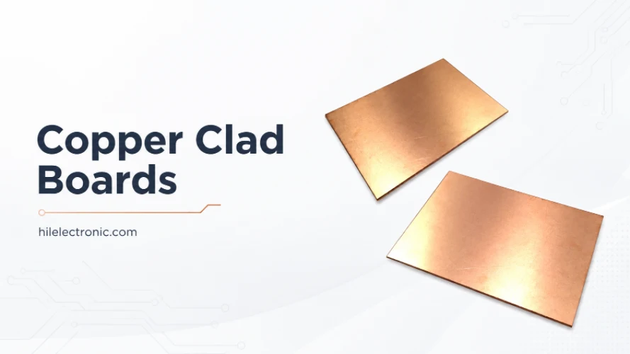
Copper Clad Boards (Copper-Clad Laminate): What They Are, Types, and How PCBs Are Made From Them
Figure 1. copper clad boards image for PCB manufacturing...
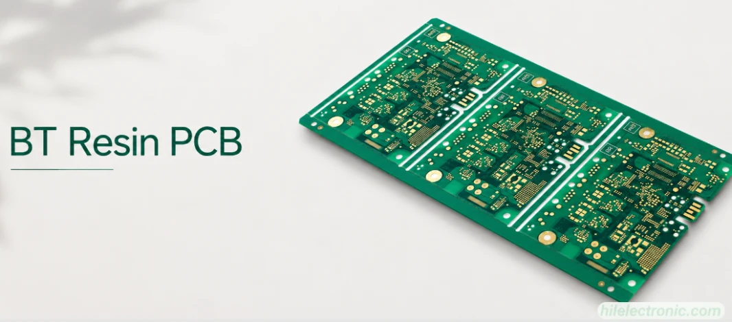
BT Resin PCB: Properties, Uses, and Fabrication Controls
Figure 1. BT resin PCB image for PCB manufacturing...
PCB Potting Services: Compounds, Process, and Design Rules
Figure 1. PCB potting services image for Highleap...
How to get a quote for PCBs
Let us run DFM/DFA analysis for you and get back to you with a report.
You can upload your files securely through our website.
We require the following information in order to give you a quote:
-
- Gerber, ODB++, or .pcb, spec.
- BOM list if you require assembly
- Quantity
- Turn time
In addition to PCB manufacturing, we offer a comprehensive range of electronic services, including PCB design, PCBA (Printed Circuit Board Assembly), and turnkey solutions. Whether you need help with prototyping, design verification, component sourcing, or mass production, we provide end-to-end support to ensure your project’s success. For PCBA services, please provide your BOM (Bill of Materials) and any specific assembly instructions. We also offer DFM/DFA analysis to optimize your designs for manufacturability and assembly, ensuring a smooth production process.