
Impedance Control in High Speed PCBs: Engineering Guide for Signal Integrity

Modern electronic systems operating at frequencies above 100MHz demand precise impedance control to maintain signal integrity and system reliability. As data transmission speeds reach multi-gigahertz ranges in applications such as 5G communications, high-speed computing, and automotive electronics, impedance control in high speed PCBs becomes a critical design requirement that directly impacts performance, electromagnetic compatibility, and overall system functionality.
What is Impedance Control?
Impedance control refers to the precise management of characteristic impedance along PCB transmission lines to ensure consistent signal propagation without distortion or reflection. Unlike simple DC resistance, characteristic impedance represents the complex relationship between voltage and current in AC transmission lines, incorporating resistance, inductance, and capacitance effects.
The characteristic impedance (Z₀) of a transmission line depends on several geometric and material factors including trace width, copper thickness, dielectric constant of the substrate material, and the distance to reference planes. In high speed PCB applications, maintaining this impedance within specified tolerances ensures optimal power transfer and minimal signal degradation.
Key Factors Influencing PCB Impedance
Geometric Parameters:
- Trace width and thickness directly affect impedance values, with wider traces producing lower impedance
- Dielectric thickness between signal traces and reference planes significantly impacts characteristic impedance
- Trace spacing in differential pairs determines differential impedance characteristics
Material Properties:
- Dielectric constant (Dk) of PCB substrates influences signal propagation speed and impedance
- Loss tangent (Df) affects signal attenuation at high frequencies
- Copper surface roughness impacts high-frequency losses and impedance stability
Why Impedance Control Matters in High Speed PCBs
Signal integrity challenges become pronounced when rise times approach nanosecond ranges or when trace lengths exceed critical electrical dimensions. Impedance mismatches create signal reflections that manifest as overshoot, undershoot, and ringing, potentially causing logic errors or system malfunctions.
Critical Applications Requiring Impedance Control:
-
DDR memory interfaces operating at multi-gigabit data rates require precise 50Ω single-ended impedance
-
High-speed serial interfaces including PCIe, SATA, and USB demand specific differential impedance values
-
RF and microwave circuits operating in gigahertz frequency ranges require controlled impedance for power transfer efficiency
-
Clock distribution networks need consistent impedance to maintain timing accuracy across the system
Signal Integrity Benefits: Proper impedance control minimizes crosstalk between adjacent traces, reduces electromagnetic interference (EMI), and ensures reliable data transmission in high-density PCB layouts. This becomes particularly critical in multi-layer boards where signal traces interact with multiple reference planes and neighboring circuits.
Types of Impedance in High Speed PCB Design
Understanding different impedance configurations enables engineers to select appropriate routing strategies for specific signal types and performance requirements.
Single-Ended Impedance
Single-ended traces carry signals referenced to a ground plane, typically requiring 50Ω impedance for most digital applications. Clock signals, address lines, and many control signals utilize single-ended routing with carefully controlled trace geometry to maintain consistent impedance.
Differential Impedance
Differential signals use paired traces carrying complementary signals, providing superior noise immunity and reduced EMI emissions. Common differential impedance requirements include 90Ω for USB interfaces, 100Ω for LVDS applications, and 85Ω for PCIe links. The spacing between differential pair traces critically affects both differential impedance and common-mode rejection.
Coplanar Waveguide Configurations
Advanced high-speed designs may employ coplanar waveguide structures where signal traces include adjacent ground traces on the same layer, providing enhanced impedance control and electromagnetic field containment for critical signal paths.
How to Achieve Impedance Control in High Speed PCB Manufacturing
Effective impedance control requires coordination between design specifications, material selection, stack-up optimization, and process control.
Stack-up Design and Material Selection
Controlled impedance begins with a well-defined stack-up. Dielectric thickness must balance target impedance and manufacturing tolerances.
-
High-performance substrates (e.g., Rogers RO4000, Megtron 6, Isola I-Speed) offer stable dielectric properties and low loss for demanding applications.
-
Enhanced FR4 remains viable below ~5 GHz when cost efficiency is prioritized. Material choice should reflect electrical performance, environment, and budget.
Trace Geometry Optimization
Accurate trace width and spacing are critical. Field solvers calculate impedance based on stack-up parameters, while tolerance analysis accounts for copper and dielectric variations.
-
Single-ended impedance: controlled by trace width vs dielectric thickness.
-
Differential impedance: trace spacing requires adjustment beyond the 3W rule to meet specific targets.
Manufacturing Process Control
Consistent processes maintain impedance accuracy.
-
Copper plating & dielectric thickness: tightly controlled for uniform geometry.
-
Verification: TDR coupon testing validates impedance against design values.
-
Statistical process control: monitors copper uniformity, dielectric stability, and etching accuracy to sustain long-term reliability.

Testing and Verification of Controlled Impedance
Comprehensive testing protocols validate impedance control implementation and ensure manufacturing consistency. Time Domain Reflectometry represents the primary measurement technique for impedance verification in production environments.
TDR Testing Methodology
TDR measurements inject fast-rise-time pulses into transmission line structures and analyze reflected signals to determine impedance variations along the trace length. This technique provides detailed impedance profiles showing discontinuities, allowing identification of manufacturing issues or design problems.
Test coupon design incorporates representative trace structures matching production circuit geometries, including single-ended traces, differential pairs, and via transitions. Coupon placement ensures measurement accuracy while minimizing impact on usable board area.
Manufacturing Quality Systems
Production testing protocols establish acceptance criteria based on design requirements and application sensitivity. Typical impedance tolerances range from ±5% for critical RF applications to ±10% for most high-speed digital circuits, with tighter control requiring more sophisticated manufacturing processes.
Documentation systems track impedance measurements, providing traceability for quality assurance and enabling correlation between process parameters and electrical performance. This data supports continuous improvement efforts and process optimization initiatives.
Common Challenges in Impedance Control
Several technical challenges can compromise impedance control implementation, requiring careful attention during design and manufacturing phases.
Material Variability and Environmental Effects
Dielectric constant variations due to resin content, glass weave effects, and moisture absorption can shift impedance values beyond acceptable tolerances. Temperature cycling and humidity exposure may cause additional impedance drift in some material systems.
Manufacturing Process Variations
Copper thickness variations from plating non-uniformity, etching process variations affecting trace width accuracy, and dielectric thickness control limitations represent primary sources of impedance deviation. Advanced process control and statistical monitoring help minimize these effects.
High-Density Design Constraints
Increasing circuit density creates routing congestion that may compromise impedance control implementation. Via transitions, layer changes, and connector interfaces introduce impedance discontinuities requiring careful design attention and potentially specialized impedance matching techniques.
Best Practices for Engineers
Successful impedance control implementation follows established engineering practices that address design, manufacturing, and verification requirements comprehensively.
Design Phase Recommendations
Early collaboration with PCB manufacturers ensures that impedance requirements align with manufacturing capabilities and material availability. Stack-up design should incorporate adequate design margins to accommodate manufacturing tolerances while meeting electrical performance targets.
Simulation and modeling tools enable impedance verification before manufacturing, reducing iteration cycles and improving first-pass success rates. Integration of electromagnetic field solvers with PCB design tools streamlines the design process and ensures consistency between calculated and manufactured impedance values.
Manufacturing Coordination
Clear specification documentation including impedance targets, measurement methods, and acceptance criteria ensures consistent manufacturing implementation. Regular communication with fabrication partners enables optimization of processes and materials for specific impedance control requirements.
Test coupon design should represent actual circuit configurations and include adequate measurement access for production testing. Documentation of measurement methods and acceptance criteria ensures consistent quality verification across different manufacturing lots.
Conclusion
Impedance control in high speed PCBs represents a fundamental requirement for modern electronic systems operating at increasing frequencies and data rates. Successful implementation requires comprehensive understanding of electromagnetic principles, material properties, manufacturing processes, and verification techniques.
Highleap Electronics Impedance Control Capabilities:
-
Advanced Manufacturing Facility – Comprehensive impedance control services for the most demanding high-speed PCB applications.
-
Extensive Material Inventory – High-performance substrates from leading suppliers (e.g., Rogers, Panasonic, Isola), enabling optimal material selection for precise electrical requirements.
-
Engineering Design Support – Stack-up optimization, impedance calculation, and simulation verification to maximize first-pass design success.
-
Process Control Systems – Advanced statistical monitoring ensures consistent impedance performance across production volumes.
-
Quality Assurance – Comprehensive TDR testing, detailed measurement documentation, and full traceability for critical applications.
-
Certified Reliability – ISO 9001 and AS9100 certified processes, meeting the stringent standards of aerospace, telecommunications, and high-performance computing industries.
Ready to optimize your high-speed PCB design with professional impedance control?
Contact our engineering team to discuss your requirements and explore how Highleap Electronics can support your next-generation electronic systems.

Recommended Posts
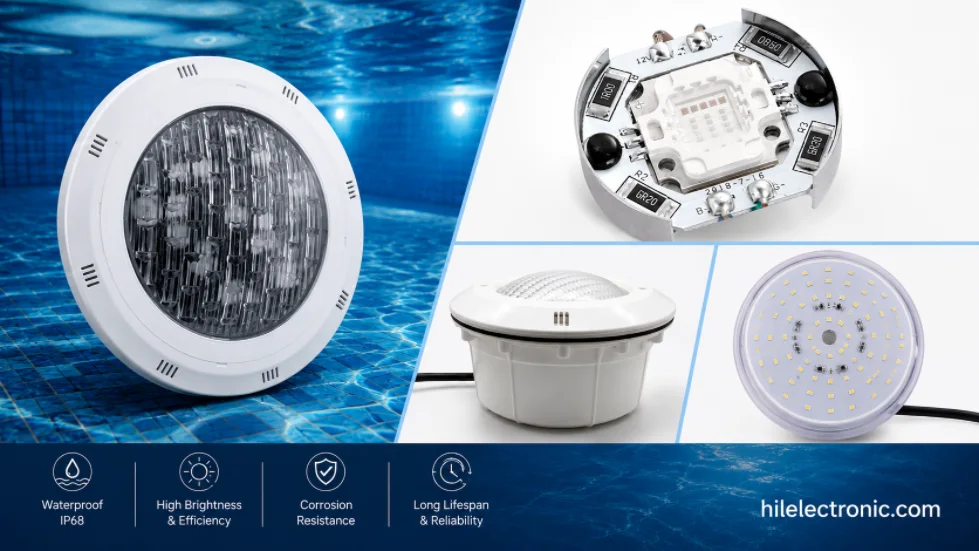
Underwater & Pool LED Light PCBs: IP68 Potted Boards, Low-Voltage Drivers & Safety
Figure 1. LED pool light PCB manufacturing reference....
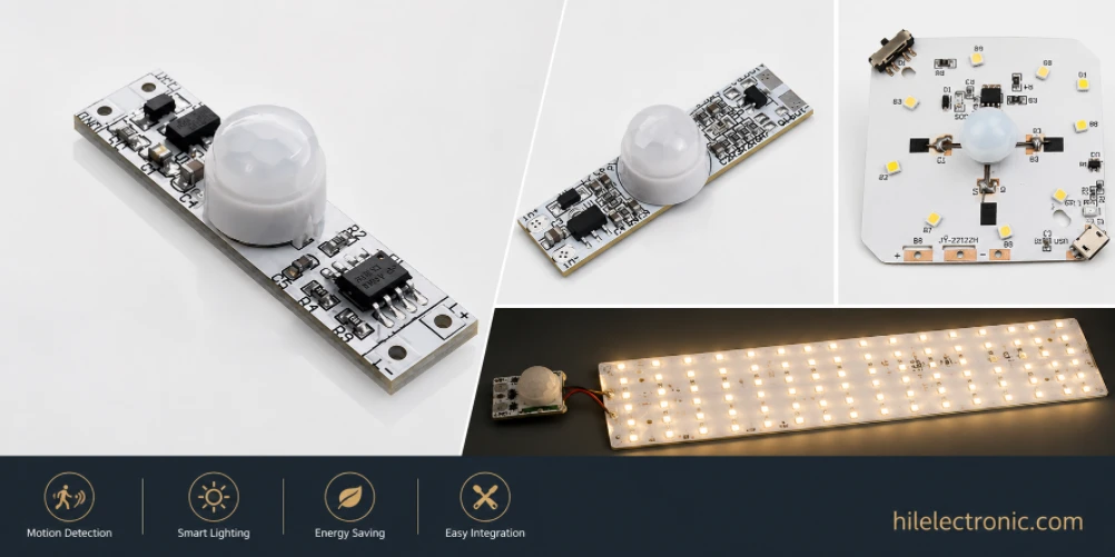
Motion Sensor & Smart LED Light PCBs: Sensor, Control, Driver & Wireless Boards
Figure 1. motion sensor LED light PCB manufacturing...

LED High Bay Light PCBs: Metal-Core Light Engines, Drivers & Turnkey Boards Built to Spec
Figure 1. LED high bay light PCB manufacturing reference....
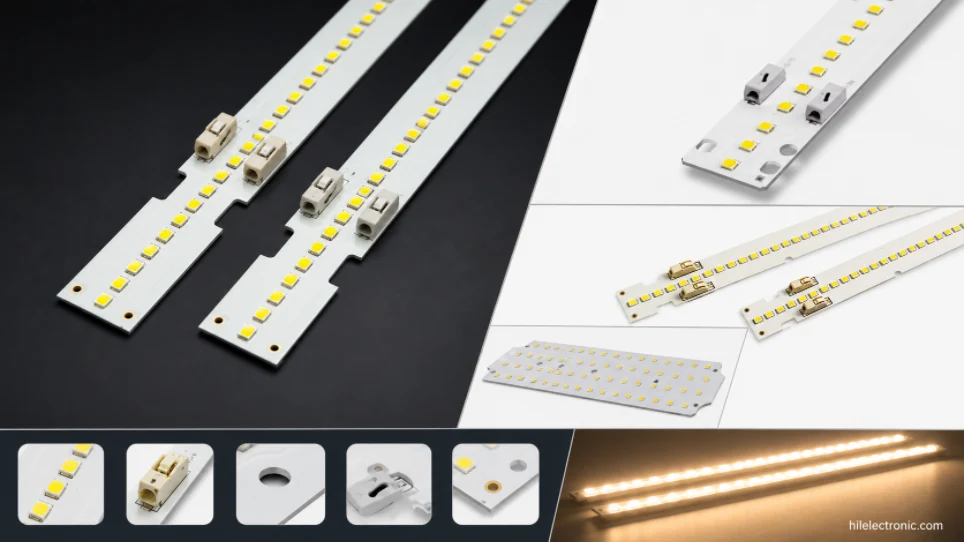
LED Linear & Strip Light PCBs: Long-Format Engines, Flexible & Rigid-Flex Boards
Figure 1. LED linear light PCB manufacturing reference....
How to get a quote for PCBs
Let‘s run DFM/DFA analysis for you and get back to you with a report. You can upload your files securely through our website. We require the following information in order to give you a quote:
-
- Gerber, ODB++, or .pcb, spec.
- BOM list if you require assembly
- Quantity
- Turn time
In addition to PCB manufacturing, we offer a comprehensive range of electronic services, including PCB design, PCBA, and turnkey solutions. Whether you need help with prototyping, design verification, component sourcing, or mass production, we provide end-to-end support to ensure your project’s success.
For PCBA services, please provide your BOM (Bill of Materials) and any specific assembly instructions. We also offer DFM/DFA analysis to optimize your designs for manufacturability and assembly, ensuring a smooth production process.