
Low PIM PCB Materials Selection: Engineering Foundation for High-Performance Antenna Systems

Introduction
Achieving low Passive Intermodulation (PIM) is critical in modern RF antenna systems where even minor nonlinearities can degrade signal quality and introduce spurious interference across adjacent frequency bands. In base station antennas, satellite communications, and distributed antenna systems, PIM-induced distortion directly impacts spectral efficiency and receiver sensitivity.
Among various design factors, the choice of circuit board materials plays a decisive role in determining PIM performance. Selecting the right Low PIM PCB materials helps engineers ensure stable impedance characteristics, minimal loss tangent, and superior intermodulation suppression in high-frequency antenna applications.
Material-level nonlinearities, rather than active component distortion, often dominate PIM behavior in passive RF assemblies, making substrate selection a fundamental engineering consideration.
Understanding PIM and Its Material Origins
Passive Intermodulation describes the phenomenon where two or more RF signals mix in passive components to generate unwanted frequencies at sum and difference products. Unlike active intermodulation produced by amplifiers or mixers, PIM arises from unintended nonlinear behavior in materials and junctions that should ideally behave linearly.
Primary Generation Mechanisms
The dominant mechanisms include nonlinear contact resistance at metal interfaces, current density variations across conductor surfaces, and localized field concentration at dielectric discontinuities. Surface oxidation layers create rectifying junctions that exhibit voltage-dependent conductivity, while ferromagnetic contamination introduces magnetic hysteresis effects that modulate current flow nonlinearly.
Material-Level Contributors
PIM originates from several substrate-related factors including copper foil surface topology, dielectric homogeneity, bonding layer consistency, and plating finish composition. Microscopic voids at copper-dielectric interfaces create tunneling barriers with nonlinear current-voltage characteristics. These material imperfections transform passive structures into weak nonlinear elements under high RF power conditions.

Key Material Properties Affecting Low PIM PCB Performance
Understanding how fundamental material characteristics influence PIM generation enables informed substrate selection. Dielectric constant stability and dissipation factor directly impact signal linearity by determining field distribution and power dissipation patterns within the substrate. Materials with tightly controlled Dk values minimize impedance variations that can concentrate current density and create localized nonlinear heating.
Surface Roughness and Conductor Quality
Copper surface topology significantly affects PIM behavior through both mechanical contact nonlinearity and current distribution effects. Rolled annealed copper with surface roughness below 2 micrometers provides substantially better PIM performance than standard electrodeposited copper with tooth-like surface profiles exceeding 5 micrometers Ra.
Conductivity and Metallic Purity
High-purity electrolytic copper with oxygen-free formulations minimizes grain boundary effects and ensures uniform current distribution. Magnetic impurities, particularly nickel-bearing interlayers or iron-based contamination, introduce hysteresis loops that modulate RF currents nonlinearly. Even trace ferromagnetic content below 0.1% can elevate PIM levels by 10-15 dB in high-power applications.
Dielectric Uniformity
Bonding resin homogeneity and ceramic filler distribution control local permittivity variations within the substrate. Non-uniform filler loading creates microscopic dielectric boundaries where charge accumulation produces field-dependent capacitance. PTFE-based systems with fluoropolymer matrices exhibit superior uniformity compared to filled epoxy systems, translating directly to lower PIM generation.
Common Low PIM PCB Materials for Antenna Designs
Material selection for low PIM applications requires balancing electrical performance, thermal management, mechanical stability, and manufacturing practicality. The following comparison highlights key substrate families used in antenna designs where PIM suppression is critical.
| Material Type | Example Products | PIM Performance | Key Characteristics |
|---|---|---|---|
| PTFE-based laminates | Rogers RT/duroid 5880, Taconic TLY-5 | Excellent (≤-160 dBc) | Ultra-low Df (0.0009), smooth rolled copper, stable Dk across temperature |
| Ceramic-filled PTFE | Rogers RO3003, RO4350B | Very Good (≤-155 dBc) | Enhanced mechanical strength, lower CTE mismatch |
| Hydrocarbon-ceramic | Rogers RO4000 series | Moderate (≤-150 dBc) | Cost-effective for mid-tier applications, easier processing |
| Metal-backed dielectrics | Aluminum or copper backplane substrates | Very Low (≤-160 dBc) | Superior thermal dissipation, dimensional stability |
| Standard FR-4 | Generic epoxy-glass | Poor (≤-135 dBc) | Not suitable for PIM-sensitive antenna designs |
PTFE-Based Substrates
PTFE matrix composites represent the benchmark for ultra-low PIM PCB materials due to their intrinsic material purity and consistent dielectric properties. The non-polar fluoropolymer structure exhibits minimal dipole relaxation losses with dissipation factors typically below 0.001, while smooth rolled copper bonding reduces interface nonlinearity.
Ceramic and Hydrocarbon Alternatives
Ceramic-loaded composites provide improved dimensional stability and lower thermal expansion compared to pure PTFE systems, though careful filler selection is essential to avoid introducing magnetic contaminants. Hydrocarbon resin systems offer processing advantages and reduced material cost while maintaining acceptable PIM performance for applications with less stringent requirements below -150 dBc.
Design and Manufacturing Considerations for Low PIM PCB Materials
Even premium substrates deliver suboptimal performance when fabrication processes introduce nonlinear junctions or surface contamination. Process control directly determines whether Low PIM PCB materials achieve their theoretical performance limits.
Critical Fabrication Requirements
Avoiding mixed-metal interfaces, particularly nickel-bearing layers beneath gold or silver finishes, eliminates galvanic junction nonlinearity that can degrade PIM by 20 dB or more. The following practices ensure optimal results:
- Finish selection – ENEPIG with palladium barrier or pure immersion silver provides superior PIM performance compared to standard ENIG processes containing magnetic nickel layers.
- Bonding integrity – Controlled lamination pressure and temperature profiles eliminate micro-voids at copper-dielectric interfaces that create capacitive discontinuities.
- Surface preparation – Plasma cleaning or chemical etching immediately before bonding removes organic residues and oxides that can create rectifying junctions.
- Tooling cleanliness – Dedicated equipment for Low PIM PCB materials processing eliminates cross-contamination from ferrous metals used in standard production.
Process Control Impact
Even the best materials can yield poor PIM performance if the fabrication process introduces non-linear joints or micro-contaminants through inadequate quality control. Rolled annealed copper with Ra values below 1.5 micrometers bonds more consistently than standard electrodeposited copper, reducing interface-related PIM generation by 5-10 dB.
Application Example: 5G Massive MIMO Antenna Module
A 64-element massive MIMO base station antenna operating at 3.5 GHz with 200W per channel input power required PIM performance below -153 dBc (referenced to +43 dBm carrier power) to meet 3GPP spurious emission limits. Initial prototypes using standard RO4350B substrates with ENIG finish achieved only -147 dBc, falling short of requirements.
Material Optimization Results
Transitioning to Rogers RT/duroid 5880 with smooth rolled copper and immersion silver finish improved PIM performance to -162 dBc, providing 9 dB margin against specifications. The material change addressed both dielectric loss tangent (reduced from 0.0037 to 0.0009) and copper surface nonlinearity. Thermal simulation confirmed adequate heat dissipation despite PTFE’s lower thermal conductivity of 0.26 W/mK, enabled by the antenna’s distributed power architecture.
Conclusion
Selecting appropriate Low PIM PCB materials forms the foundation of reliable high-performance antenna systems operating in demanding RF environments. Material integrity directly influences intermodulation behavior through surface topology, dielectric uniformity, and metallic purity. The interaction between substrate properties, copper surface quality, and plating finish composition determines whether passive structures remain truly linear under high-power RF conditions.
Highleap Electronics provides comprehensive low PIM PCB solutions optimized for demanding antenna applications:
- Advanced material selection – Supporting PTFE-based laminates, ceramic-filled composites, and metal-backed substrates with verified PIM performance below -160 dBc.
- Precision surface finishing – ENEPIG and immersion silver processes with controlled plating parameters to eliminate magnetic contamination and junction nonlinearity.
- Controlled manufacturing environment – Dedicated tooling and contamination-free fabrication processes specifically designed for PIM-critical applications.
- Engineering support – Material selection guidance, stack-up optimization, and thermal analysis to achieve superior performance in base station antennas, satellite communications, and distributed antenna systems.

Recommended Posts

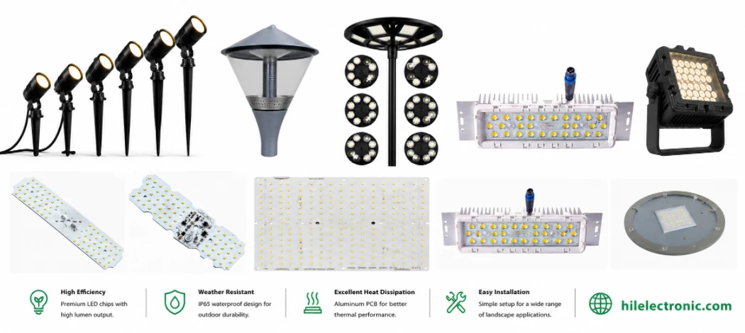
LED Garden Light PCB Manufacturing & Assembly by Highleap Electronics
Figure 1. LED garden light PCB production and assembly...
LED Landscape Light PCB Manufacturing — Uplight, Well Light & Underwater Engines
Figure 1. LED landscape light PCB production and assembly...
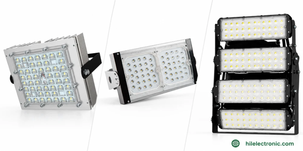
LED Parking Lot Light PCB Manufacturing & Assembly by Highleap Electronics
Figure 1. LED parking lot light PCB production and...
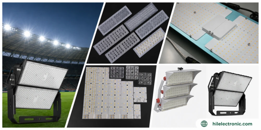
LED Stadium Light PCB Manufacturing — Very-High-Power Engines & Flicker-Free Drivers
Figure 1. LED stadium light PCB production and assembly...
How to get a quote for PCBs
Let‘s run DFM/DFA analysis for you and get back to you with a report. You can upload your files securely through our website. We require the following information in order to give you a quote:
-
- Gerber, ODB++, or .pcb, spec.
- BOM list if you require assembly
- Quantity
- Turn time
In addition to PCB manufacturing, we offer a comprehensive range of electronic services, including PCB design, PCBA, and turnkey solutions. Whether you need help with prototyping, design verification, component sourcing, or mass production, we provide end-to-end support to ensure your project’s success.
For PCBA services, please provide your BOM (Bill of Materials) and any specific assembly instructions. We also offer DFM/DFA analysis to optimize your designs for manufacturability and assembly, ensuring a smooth production process.