
RF Simulation Tools for PCB Design: A Comprehensive Guide

Introduction
High-frequency circuit design demands precision that traditional PCB layout approaches cannot deliver. As operating frequencies increase, wavelengths shrink to dimensions comparable to PCB traces, making electromagnetic effects dominant factors in circuit performance. RF simulation tools for PCB design have become essential for predicting signal behavior, optimizing impedance matching, and eliminating costly prototype iterations.
Selecting appropriate RF simulation and modeling tools directly impacts design success. Engineers must balance simulation accuracy, workflow integration, and computational efficiency while addressing frequency-dependent effects such as dielectric losses, parasitic coupling, and resonance modes. This article examines leading simulation platforms and their optimal applications in RF PCB development.
Importance of Simulation in RF PCB Design
Why RF Designs Require Simulation
RF PCB simulation addresses challenges invisible to DC and low-frequency design rules. Electromagnetic coupling between adjacent traces, signal reflection at impedance discontinuities, and substrate losses all degrade circuit performance in ways that require field-level analysis. Designers use simulation to optimize transmission line dimensions, predict return loss across frequency bands, and verify that layout geometries meet electrical specifications before fabrication.
Circuit-Level Simulation
Circuit-level tools analyze RF networks using lumped and distributed element models. Engineers verify amplifier stability, filter response, and matching network performance through S-parameter analysis and harmonic balance methods. These simulations identify component sensitivities and optimize circuit topologies before physical implementation.
Electromagnetic Field Simulation
EM simulation solves Maxwell’s equations across three-dimensional PCB structures. This approach captures distributed effects in transmission lines, discontinuities at vias and bends, and mutual coupling between circuit elements. Electromagnetic modeling provides the accuracy necessary for designs above several gigahertz where physical dimensions approach wavelength scales.
System-Level Modeling
System-level RF modeling integrates circuit blocks, propagation paths, and interference sources into unified simulations. This analysis evaluates end-to-end performance including antenna efficiency, receiver sensitivity, and spurious emission levels. System modeling guides architecture decisions and validates compliance with communication standards.

Overview of Leading RF Simulation Tools
Keysight ADS (Advanced Design System)
ADS excels at circuit and system-level RF simulation with comprehensive libraries for active and passive components. The platform provides S-parameter analysis, harmonic balance for nonlinear circuits, and transient envelope simulation for modulated signals. Integrated Momentum solvers enable planar electromagnetic analysis directly within the circuit environment, allowing engineers to co-simulate distributed structures with lumped elements.
ADS serves as the primary platform for RF front-end design including filters, amplifiers, and mixers. Its strength lies in rapid iteration between schematic capture and measurement-based validation, with built-in optimization routines that tune circuit parameters to meet performance specifications.
Ansys HFSS
HFSS delivers full-wave 3D electromagnetic simulation using finite element methods. The solver handles complex geometries including multilayer PCB stackups, wire bonds, and electromagnetic shielding structures. HFSS accurately predicts field distributions, radiation patterns, and coupling mechanisms in structures where current paths and charge distributions cannot be approximated by simplified models.
Applications span high-frequency PCB interconnects, antenna integration, and package-level parasitic extraction. HFSS becomes essential above 10 GHz where skin depth, surface roughness, and dielectric dispersion significantly impact signal integrity. The platform’s adaptive meshing ensures convergence while managing computational resources for electrically large problems.
CST Studio Suite
CST provides multiple solver technologies within a unified interface, including time-domain, frequency-domain, and eigenmode methods. This flexibility allows engineers to select the most efficient approach for each structure type. Time-domain solvers efficiently characterize broadband responses, while frequency-domain methods excel at resonant structures and high-Q filters.
The platform addresses antenna arrays, EMC/EMI compliance analysis, and package-level coupling between power delivery networks and signal paths. CST’s strength in handling electrically large structures makes it valuable for system-level electromagnetic compatibility studies and co-simulation of mechanical and thermal effects with electromagnetic behavior.
Cadence AWR Microwave Office
AWR Microwave Office targets RF and microwave circuit designers with streamlined workflows for filter synthesis, amplifier design, and module-level integration. The platform emphasizes bidirectional links between schematic and layout, enabling real-time electromagnetic verification as geometries evolve. Integrated AXIEM planar EM solver provides rapid analysis of microstrip and stripline structures.
AWR suits rapid prototyping environments where designers iterate quickly between circuit topology and physical implementation. The tool’s templated design flows accelerate common tasks such as impedance matching network synthesis and coupled-line filter realization.
Altium Designer with Integrated RF Simulation
Altium Designer incorporates basic RF simulation capabilities within its unified PCB design environment. While less comprehensive than dedicated RF platforms, Altium provides sufficient analysis for moderate frequency applications and educational purposes. The integrated approach reduces tool switching overhead for designs where RF functionality represents one aspect of a larger mixed-signal system.
Altium serves entry-level RF development and projects where simulation validates basic transmission line properties rather than exploring subtle electromagnetic phenomena. The platform’s value lies in workflow continuity rather than simulation depth.
Comparative Analysis: Strengths and Use Cases
The choice of RF simulation tools depends on frequency range, structural complexity, and required accuracy. Projects demanding sub-0.1 dB precision in insertion loss require full-wave electromagnetic analysis, while conceptual designs benefit from circuit-level tools that explore topology alternatives rapidly.
| Software | Core Strengths | Typical Applications | Design Stage |
|---|---|---|---|
| Keysight ADS | Circuit and system modeling, comprehensive component libraries, measurement integration | Filter design, power amplifiers, RF front-end modules, wireless transceivers | Concept validation, circuit optimization |
| Ansys HFSS | High-accuracy 3D EM simulation, complex geometry handling, material modeling | Antenna design, PCB stackup optimization, package parasitic extraction | Physical structure design, detailed analysis |
| CST Studio Suite | Multi-solver flexibility, time/frequency domain analysis, EMC/EMI prediction | Antenna arrays, system-level EMI, package coupling, co-simulation | Comprehensive verification, compliance validation |
| Cadence AWR | Rapid schematic-to-layout iteration, filter synthesis, planar EM analysis | RF modules, passive component design, quick prototyping | Fast iteration, design exploration |
| Altium Designer | Integrated PCB workflow, basic transmission line analysis, accessibility | Entry-level RF, mixed-signal boards, educational projects | Initial validation, moderate frequency ranges |
Integration of Simulation into PCB Design Workflow
Material Parameter Definition
Accurate RF PCB simulation begins with precise material characterization. Engineers input substrate dielectric constant, loss tangent, and frequency-dependent behavior for each layer in the stackup. Copper surface roughness models account for skin effect losses that become dominant above several gigahertz. These parameters transform geometric layouts into accurate electromagnetic models that predict fabricated performance.
Stackup and Impedance Modeling
Transmission line simulation verifies that trace geometries achieve target impedance across the operating bandwidth. Multi-layer stackups require analysis of reference plane return paths, via transitions between layers, and ground plane discontinuities. Impedance verification during layout prevents reflection-induced signal degradation that compromises link budgets in RF systems.
Post-Layout Verification
After completing physical layout, engineers extract electromagnetic models of critical paths and re-simulate circuit performance with distributed effects included. This verification stage identifies layout-induced resonances, unintended coupling, and impedance mismatches that schematic-level simulation cannot predict. Iteration between layout modification and EM re-analysis continues until performance meets specifications.
Closing the Design-to-Manufacturing Loop
Simulation results guide fabrication process selection and tolerance specification. Manufacturers use impedance targets derived from simulation to control dielectric thickness and trace dimensions. Post-fabrication measurements validate simulation accuracy and refine material models for subsequent designs, creating a continuous improvement cycle between prediction and physical implementation.
Future Trends in RF Simulation Tools
AI-Assisted Simulation and Optimization
Machine learning algorithms are being integrated into RF simulation platforms to accelerate design space exploration. AI-assisted simulation predicts optimal component values and layout geometries based on training data from previous designs, reducing the number of electromagnetic solves required to achieve performance targets. Neural network-based surrogate models approximate computationally expensive EM simulations, enabling real-time optimization during interactive layout sessions.
Cloud-Based RF Modeling
Cloud computing infrastructure enables parallelization of RF simulations across distributed resources, dramatically reducing solve times for electromagnetically large problems. Cloud-based RF modeling platforms provide access to high-performance computing without local hardware investment, democratizing advanced simulation capabilities for small design teams. Collaborative cloud environments allow distributed engineering groups to share models and results in real-time.
Multi-Physics Coupled Analysis
Modern RF systems require simultaneous consideration of electromagnetic, thermal, and mechanical effects. Multi-physics simulation platforms couple EM solvers with thermal analysis to predict temperature-dependent performance shifts and mechanical stress analysis to evaluate reliability under vibration. This integrated approach addresses power amplifier thermal management, package
Conclusion
RF simulation tools have become indispensable for modern high-frequency PCB design, with each platform offering distinct advantages for specific applications:
- Keysight ADS – Comprehensive circuit and system-level analysis ideal for RF front-end, amplifier, and filter design.
- Ansys HFSS – Unmatched 3D electromagnetic accuracy for complex geometries, antennas, and high-frequency packaging.
- CST Studio Suite – Multi-solver flexibility supporting EMC/EMI, signal coupling, and multi-physics simulation.
- Cadence AWR – Rapid design iteration and optimization for microwave circuits and integrated RF modules.
- Altium Designer – Integrated PCB workflow with essential RF simulation capabilities for early design validation.
Selection criteria should focus on:
- Frequency range – Ensure solver accuracy and model resolution align with target operating frequencies.
- Geometric complexity – Match tool capability to antenna, cavity, or multi-layer structure intricacy.
- Simulation accuracy – Balance computational efficiency against required precision in S-parameters and field distribution.
- Design integration – Optimize workflow continuity between schematic, layout, and manufacturing environments.
Engineers who leverage appropriate RF simulation and modeling tools gain predictive insight into electromagnetic behavior, reduce prototype iterations, and deliver reliable high-frequency designs.
Highleap Electronics provides advanced RF PCB fabrication and design support, collaborating with engineers using leading simulation platforms to ensure high-frequency performance and manufacturing reliability. Our process capabilities support controlled impedance structures, low-loss materials, and precision geometries required by demanding RF applications.

Recommended Posts

PCB Soldering Machine Types: Reflow, Wave, and Selective Equipment
Figure 1. PCB soldering machine types image for Highleap...
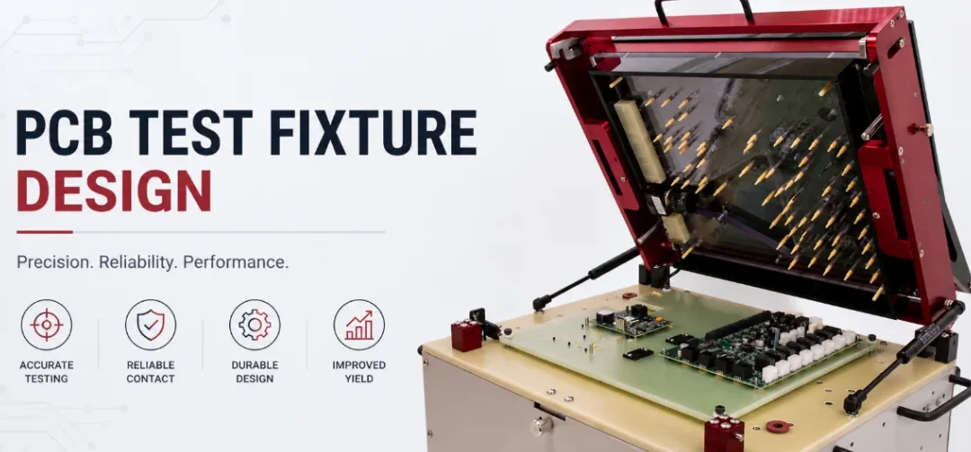
PCB Test Fixture Design: Bed-of-Nails, Flying Probe, and DFT
Figure 1. PCB test fixture design image for Highleap...

Clean Flux vs No-Clean Flux: Residue, Cleaning, and PCB Reliability
Figure 1. clean flux vs no-clean flux image for Highleap...
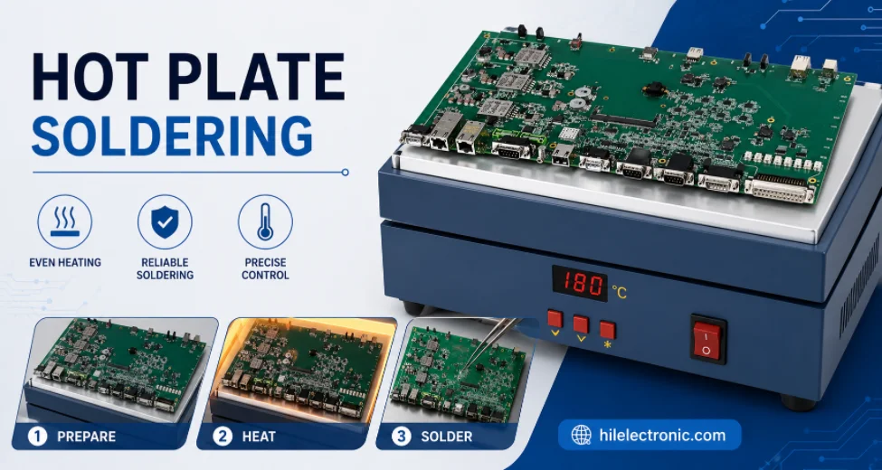
Hot Plate Soldering: Process, Limits, and Reflow Comparison
Figure 1. hot plate soldering image for Highleap...
How to get a quote for PCBs
Let‘s run DFM/DFA analysis for you and get back to you with a report. You can upload your files securely through our website. We require the following information in order to give you a quote:
-
- Gerber, ODB++, or .pcb, spec.
- BOM list if you require assembly
- Quantity
- Turn time
In addition to PCB manufacturing, we offer a comprehensive range of electronic services, including PCB design, PCBA, and turnkey solutions. Whether you need help with prototyping, design verification, component sourcing, or mass production, we provide end-to-end support to ensure your project’s success.
For PCBA services, please provide your BOM (Bill of Materials) and any specific assembly instructions. We also offer DFM/DFA analysis to optimize your designs for manufacturability and assembly, ensuring a smooth production process.