
High Frequency PCB Design: A Practical Engineering Guide

Introduction
High frequency PCB design has become essential in modern electronic systems, from 5G infrastructure and automotive radar to satellite communications and IoT gateways. As operating frequencies push beyond several gigahertz, the fundamental challenge shifts from simple circuit connectivity to maintaining signal integrity and minimizing transmission losses across the board.
The key to successful high frequency PCB design lies in understanding that signals no longer behave as simple voltages on conductors but propagate as electromagnetic waves through carefully controlled transmission media. This article provides practical engineering guidance across six critical areas: material selection, stack-up architecture, impedance control, layout optimization, electromagnetic compatibility, and manufacturing considerations. Whether you are designing RF PCBs for wireless communications or high-speed digital systems, these principles will help you achieve reliable, low-loss signal transmission.
Understanding High Frequency Behavior on PCB
Electromagnetic Wave Propagation
At high frequencies, signal transmission fundamentally changes from conductor-based voltage propagation to electromagnetic wave propagation through the PCB substrate. This shift requires engineers to treat every trace as a transmission line with characteristic impedance, propagation delay, and frequency-dependent losses. The PCB ceases to be a simple mounting platform and becomes an integral part of the RF signal path.
Critical Material Properties
Three material parameters dominate high frequency signal performance: dielectric constant (Dk), dissipation factor (Df), and copper surface roughness. The dielectric constant determines signal velocity and impedance, while the dissipation factor directly translates to signal loss through the substrate. Copper roughness becomes increasingly important above 1 GHz, where skin effect concentrates current flow near conductor surfaces, making surface texture a significant contributor to insertion loss.
Key High Frequency Effects
Skin effect forces current to flow in an increasingly thin layer near the conductor surface as frequency rises, effectively increasing resistance and signal loss. Dielectric loss occurs as the alternating electric field causes molecular friction within the substrate material, converting signal energy to heat. Crosstalk between adjacent traces intensifies at high frequencies due to both capacitive and inductive coupling, requiring careful spacing and shielding strategies to maintain signal integrity.

High-Frequency PCB
Material Selection for High Frequency PCB
Beyond Standard FR4
Standard FR4 laminate, while cost-effective for general applications, presents significant limitations for high frequency PCB design. Its relatively high dissipation factor (typically 0.02) and variable dielectric constant (4.2-4.5 with frequency and temperature dependence) make it unsuitable for precision RF applications above 1-2 GHz. High frequency laminates from Rogers, Taconic, Isola, and Panasonic offer tightly controlled electrical properties specifically engineered for RF signal transmission.
Performance Comparison
Rogers 4350B represents a widely adopted compromise between performance and manufacturability, offering a stable Dk of 3.48 and low Df of 0.0037 while maintaining compatibility with standard FR4 processing temperatures. Pure PTFE-based materials like Rogers 3003 provide even lower losses (Df of 0.0013) but require specialized processing. The table below illustrates key differences:
| Material | Dk @ 10GHz | Df @ 10GHz | Thermal Coefficient |
|---|---|---|---|
| FR4 | 4.3 | 0.020 | High variance |
| Rogers 4350B | 3.48 | 0.0037 | ±50 ppm/°C |
| Rogers 3003 | 3.00 | 0.0013 | -24 ppm/°C |
Selection Criteria
Material selection for high frequency PCB design must balance electrical performance, thermal stability, and manufacturing compatibility. Applications requiring operation across wide temperature ranges demand materials with low coefficient of thermal expansion (CTE) to prevent impedance shifts and mechanical stress. Cost optimization often leads to hybrid stack-ups combining high-performance materials on RF signal layers with standard FR4 for non-critical layers.
Stack-up Design and Impedance Control
Layer Configuration Strategy
Controlled impedance transmission requires careful pairing of signal layers with reference planes. Each high frequency signal layer should have an adjacent ground or power plane at a precisely controlled distance, forming either microstrip (outer layer) or stripline (inner layer) transmission structures. This signal-ground coupling provides the return path necessary for electromagnetic wave propagation and shields signals from adjacent layers.
Impedance Calculation and Control
Characteristic impedance depends on trace width, substrate thickness, and dielectric constant according to established transmission line equations. For a microstrip line, impedance decreases with wider traces and thinner substrates. Achieving standard impedances like 50Ω for RF systems or 100Ω for differential pairs requires careful dimensional control, typically ±10% tolerance. Modern impedance calculators like Polar SI9000 or integrated tools in advanced EDA software enable accurate modeling before fabrication.
Microstrip versus Stripline
Microstrip transmission lines place the signal trace on the outer layer with a single reference plane below, offering easier impedance control and lower cost but exposing the signal to electromagnetic radiation. Stripline structures sandwich the signal between two reference planes, providing superior EMI shielding and more stable impedance across frequency, though at the expense of higher losses due to longer return path and more complex fabrication.
Layout and Routing Best Practices
Transmission Path Optimization
High frequency PCB design demands the shortest practical signal paths with minimal discontinuities. Every via, connector, and direction change introduces impedance variations that cause reflections and signal degradation. Engineers should route RF traces as continuous transmission lines with constant cross-section, avoiding unnecessary meanders or length matching serpentines that increase losses without providing functional benefit.
Corner and Transition Management
Sharp 90-degree corners create impedance discontinuities and increase radiated emissions at high frequencies. Standard practice specifies 45-degree chamfered corners or curved traces with radius at least three times the trace width. When vias are unavoidable, back-drilling or via stubs removal prevents resonances that cause severe reflections at specific frequencies. Transition between layers requires careful via design with surrounding ground vias to maintain controlled impedance.
Return Path Continuity
The ground plane beneath a high frequency signal trace carries the return current, and any interruption forces this current to detour, creating inductance and potential EMI issues. Split ground planes, cutouts, or plane transitions under signal traces must be avoided. When signals must cross plane boundaries, stitching capacitors or closely spaced ground vias provide a low-impedance return path at the crossing point.
Differential Pair Routing
Differential signaling provides inherent noise immunity and reduced EMI, but requires matched trace lengths and consistent spacing throughout the routing path. Length mismatch should remain below 5 mils for most high-speed differential applications, while spacing must be maintained to achieve the target differential impedance. Avoid routing differential pairs over plane splits or near board edges where asymmetry degrades common-mode rejection.
Managing Crosstalk, EMI and Grounding
Crosstalk Prevention
Capacitive and inductive coupling between adjacent traces increases dramatically with frequency, making crosstalk a primary concern in high frequency PCB design. The 3W rule (spacing equals three times trace width) provides baseline isolation for parallel traces. Critical RF signal paths require additional separation or ground trace shielding. When traces must run parallel for extended distances, routing on different layers with a ground plane between provides superior isolation.
Ground Plane Strategy
A continuous, uninterrupted ground plane serves as the foundation for effective high frequency PCB design, providing both the signal return path and electromagnetic shielding. Multiple ground planes in the stack-up should be connected with numerous vias distributed across the board, creating a low-impedance ground network. Avoid splitting ground planes into isolated islands, which creates uncontrolled loop antennas and increases radiated emissions.
Via Fencing and Shielding
Rows of grounded vias placed along sensitive signal boundaries create “via fences” that contain electromagnetic fields and reduce coupling between board regions. Via spacing should not exceed one-tenth wavelength at the highest operating frequency. For critical RF sections, complete shielded compartments can be created using via walls combined with grounded copper pours, effectively isolating sensitive circuits from digital noise sources.
Power Distribution
Power supply noise couples directly into RF signal paths through the shared substrate. Star or tree power distribution topologies minimize common impedance, while distributed decoupling capacitors at multiple values provide low-impedance paths across the full frequency spectrum. Physical separation of analog, digital, and RF power domains with ferrite beads or LC filters prevents high-frequency noise propagation between subsystems.

High Frequency Circuit Board Manufacturing
Manufacturing and Assembly Considerations
Copper Surface Management
Copper foil roughness significantly impacts high frequency signal loss through increased effective resistance and dielectric loss from field penetration into surface irregularities. Standard electrodeposited copper with roughness profiles designed for adhesion becomes problematic above several gigahertz. Specifying rolled copper foil or reverse-treated foil reduces surface roughness by 50% or more, directly improving insertion loss performance in high frequency PCB designs.
Surface Finish Selection
Electroless nickel immersion gold (ENIG) provides excellent solderability and wire bonding capability but introduces a nickel layer with higher resistivity than copper. For frequencies above 3-5 GHz, immersion silver or organic solderability preservative (OSP) finishes maintain lower signal loss by avoiding the nickel barrier. The choice depends on assembly requirements, environmental exposure, and shelf-life considerations balanced against electrical performance targets.
Lamination and Drilling Precision
High frequency laminates require controlled lamination cycles with precise temperature profiles to achieve target dielectric thickness and minimize voids that create impedance variations. Drilling accuracy becomes critical for maintaining via stub lengths and pad-to-trace transitions. Laser drilling for microvias and sequential lamination build-up techniques enable finer features necessary for impedance control in dense, high-frequency circuit layouts.
Assembly Impact on Performance
Component placement directly affects transmission line performance, with pad geometries and solder joint profiles creating impedance discontinuities. Excessive solder paste thickness or fillet size can detune RF matching networks or shift resonant frequencies. High frequency PCB assembly requires careful process control, with recommended paste thicknesses and reflow profiles validated for the specific substrate materials used.
Testing and Validation
Time Domain Reflectometry
Time domain reflectometry (TDR) provides immediate visualization of impedance variations along a transmission line by measuring reflections from discontinuities. A TDR trace reveals connector transitions, via stubs, and trace width changes as impedance steps or peaks. This technique validates controlled impedance fabrication and identifies specific locations of design or manufacturing issues before RF testing begins.
Frequency Domain Characterization
Vector network analyzers (VNA) measure insertion loss and return loss across frequency ranges, quantifying signal attenuation and impedance matching performance. Insertion loss should follow predicted values from material datasheets and simulation models, while return loss indicates how well the transmission system impedance matches the source and load. De-embedding techniques using calibration standards remove test fixture effects to isolate the actual PCB performance.
Acceptance Criteria
High frequency PCB validation requires comparison against specific performance targets derived from system requirements. Return loss better than -10 dB ensures less than 10% of signal power reflects, while insertion loss budgets allocate acceptable attenuation across frequency bands. Phase matching between channels, group delay flatness, and isolation between ports provide additional metrics for multi-channel RF systems.
Conclusion
Successful high frequency PCB design integrates material science, electromagnetic theory, and manufacturing practicality. The progression from low-loss material selection through stack-up design, impedance control, and layout optimization creates the foundation for reliable RF signal transmission. As wireless systems continue pushing toward millimeter-wave frequencies, mastering these fundamentals becomes increasingly critical to product success.
Highleap Electronics provides comprehensive high frequency PCB capabilities:
- Advanced material support – Rogers, Taconic, and hybrid stack-ups with controlled dielectric properties for RF applications
- Precision impedance control – Tight tolerance fabrication with impedance testing and validation at specified frequencies
- Design for manufacturing analysis – Engineering team reviews layouts for optimal high frequency performance and manufacturability
- Complete assembly services – RF-optimized processes including controlled solder application and validated reflow profiles
Contact our engineering team to discuss your specific high frequency PCB requirements and learn how our expertise can accelerate your development timeline for RF, microwave, and high-speed digital projects.

Recommended Posts
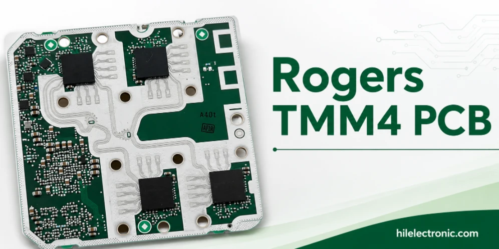
Rogers TMM4 PCB Manufacturer for Compact Microwave Filters
TMM4 is most useful when a microwave circuit must become...
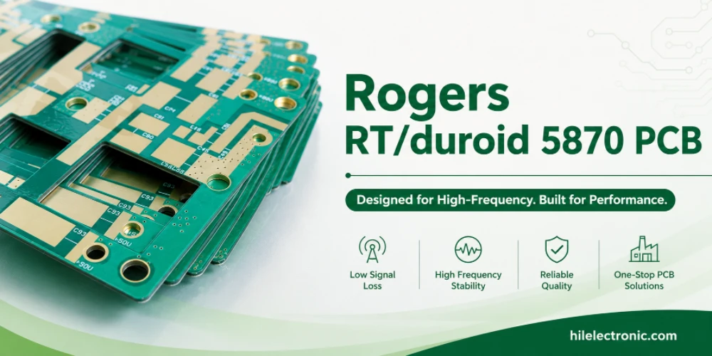
RT/duroid 5870 PCB Manufacturer for Low-Loss PTFE RF Circuits
RT/duroid 5870 is chosen when the RF path needs low loss,...
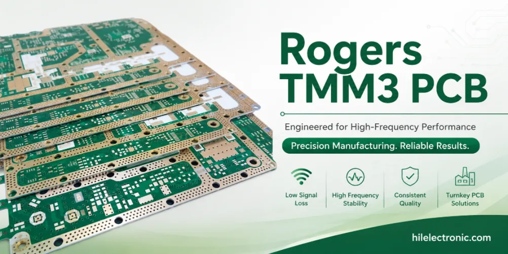
Rogers TMM3 PCB Manufacturer for Mechanical RF Modules
TMM3 is selected when an RF circuit must behave as part of...
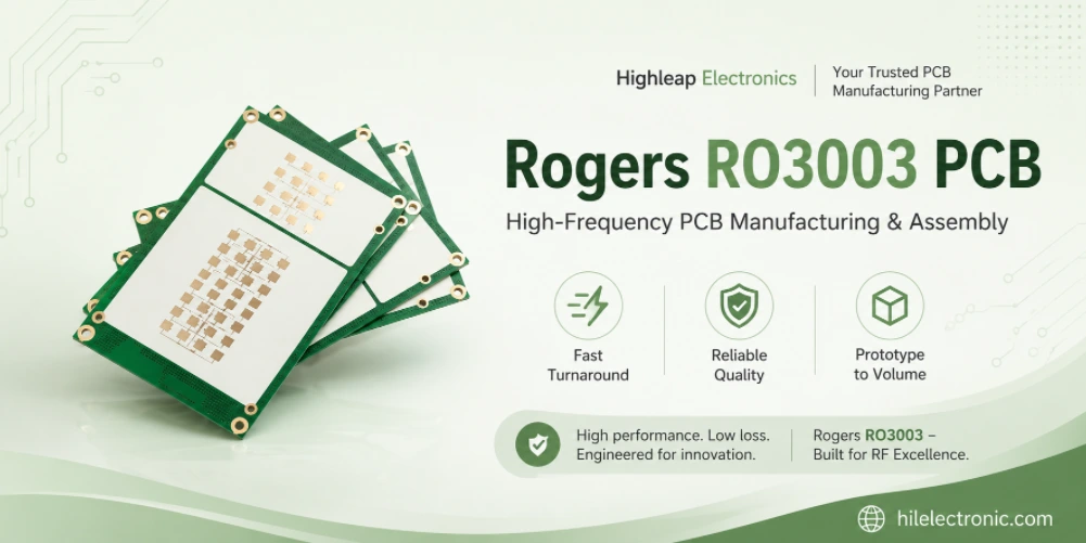
Rogers RO3003 PCB Manufacturer for Automotive Radar and mmWave Modules
A 77 GHz radar board is purchased as a working sensor...
How to get a quote for PCBs
Let‘s run DFM/DFA analysis for you and get back to you with a report. You can upload your files securely through our website. We require the following information in order to give you a quote:
-
- Gerber, ODB++, or .pcb, spec.
- BOM list if you require assembly
- Quantity
- Turn time
In addition to PCB manufacturing, we offer a comprehensive range of electronic services, including PCB design, PCBA, and turnkey solutions. Whether you need help with prototyping, design verification, component sourcing, or mass production, we provide end-to-end support to ensure your project’s success.
For PCBA services, please provide your BOM (Bill of Materials) and any specific assembly instructions. We also offer DFM/DFA analysis to optimize your designs for manufacturability and assembly, ensuring a smooth production process.