
RF PCB Tolerance: Precision Manufacturing for High-Frequency Performance

Introduction
In RF PCB manufacturing, dimensional precision directly determines circuit performance. High-frequency signals are extremely sensitive to geometric variations, with even micron-level deviations in trace width, dielectric thickness, or copper weight affecting impedance matching and signal integrity. At frequencies above 3 GHz, RF PCB tolerance specifications that would be acceptable in digital circuits can cause significant insertion loss, phase errors, and return loss degradation.
Achieving tight tolerance control requires understanding the relationship between physical dimensions and electrical performance, then implementing rigorous process controls throughout fabrication. This article examines how precision manufacturing techniques maintain the dimensional accuracy essential for reliable RF circuit operation.
The Role of RF PCB Tolerance in Circuit Performance
Manufacturing variations translate directly into electrical performance shifts in RF circuits. A 10-micron change in trace width alters characteristic impedance, creating reflections that degrade signal power transfer. When dielectric thickness varies by even 5%, the resulting impedance shift can move a 50-ohm transmission line outside acceptable matching windows.
At RF frequencies, wavelengths become comparable to PCB feature sizes, making circuits sensitive to dimensional precision. A phase velocity change of 2% from dielectric thickness variation translates to significant electrical length error in quarter-wave structures. Above 10 GHz, RF PCB tolerance deviations that cause negligible effects at lower frequencies produce insertion loss variations exceeding 0.5 dB per inch of trace length.
Key Manufacturing Tolerances in RF PCBs
Dielectric Thickness Control
Dielectric layer thickness directly controls impedance and propagation velocity. Standard FR-4 processes achieve ±10% thickness tolerance, but RF applications typically require ±5% or tighter control. A 100-micron dielectric variation in a 250-micron layer shifts microstrip impedance by approximately 4 ohms, enough to cause significant mismatch.
High-frequency laminates from Rogers or Taconic offer better thickness consistency, with premium grades achieving ±3% tolerance through controlled resin content and press cycles.
Copper Thickness Variation
Copper weight affects both trace resistance and effective trace width after etching. Standard half-ounce copper varies by ±10%, translating to 3-4 micron thickness differences. This variation alters the width-to-height ratio of transmission lines, shifting impedance and changing conductor loss.
Electrodeposited copper provides tighter control than rolled copper, with precision plating processes achieving ±5% thickness uniformity critical for maintaining consistent RF PCB tolerance across panel area.
Layer Registration Accuracy
Multilayer RF PCBs require precise alignment between signal layers and ground planes. Registration errors of 75 microns or more cause impedance discontinuities where vias transition between layers. Advanced manufacturing uses optical fiducial alignment and precision lamination presses to achieve ±50-micron registration.
Critical designs specify ±25-micron alignment for millimeter-wave circuits where via transitions must maintain controlled impedance throughout the vertical path.
Etching Precision
Photolithographic etching determines final trace geometry. Standard subtractive etching produces ±20% line width variation due to undercut and sidewall angle. For a 200-micron trace, this 40-micron variation changes microstrip impedance by 3-5 ohms.
Controlled-depth etching reduces variation to ±10%, while modified semi-additive processes achieve ±10-micron absolute tolerance. The etch compensation applied during artwork generation must account for copper thickness and panel position.
Via and Drill Tolerance
Through-hole and blind via dimensions affect both DC resistance and RF impedance. Mechanical drilling achieves ±75-micron diameter tolerance, while laser drilling provides ±10-micron precision for microvias. Via barrel thickness variation from electroplating creates impedance discontinuities, particularly in controlled-impedance via structures.

Stack-up and Dielectric Uniformity for RF PCB Tolerance
Laminate stack-up consistency determines whether manufactured boards match design impedance targets. The press cycle controls resin flow, consolidation pressure, and temperature ramp rates that affect final dielectric thickness. Prepreg resin content variations of ±5% can shift pressed thickness by 15-20 microns.
Material Selection Impact
Material choice directly impacts achievable RF PCB tolerance specifications. PTFE-based laminates from Rogers RO4000 series offer thickness tolerances of ±0.5 mil (±12.7 microns) in standard grades, with precision grades reaching ±0.3 mil. Hydrocarbon ceramics like RO4350B provide dimensional stability across temperature, maintaining thickness within ±2% from -40°C to +140°C.
The dielectric constant tolerance of these materials, typically ±2%, combines with thickness control to maintain impedance within specification.
Press Process Optimization
Press process optimization uses controlled heating rates and dwell times to achieve uniform resin cure. Multi-opening tooling plates and precisely machined press platens distribute pressure evenly across panel area, minimizing thickness gradients. Monitoring press parameters with statistical process control identifies drift before parts fall outside tolerance specifications.
Process Precision and Measurement Techniques
Manufacturing verification begins with incoming material inspection using calibrated micrometers and optical measurement systems. Laser scanning measures copper foil thickness at multiple points to establish baseline uniformity. Cross-sectional analysis of laminate samples verifies dielectric thickness and resin-to-glass ratio before production begins.
In-Process Monitoring Methods
In-process monitoring uses impedance test coupons placed on panel edges. Time-domain reflectometry measures fabricated impedance against design targets, with results fed back to adjust etch compensation and press parameters. Automated optical inspection systems verify trace width at multiple locations, detecting process drift before entire panels fall outside RF PCB tolerance specifications.
Statistical Process Control
Statistical process control establishes capability indices for critical parameters. Process capability (Cp) above 1.33 indicates that natural process variation fits well within specification limits, while Cpk accounts for process centering. Tracking these metrics for dielectric thickness, copper weight, and registration accuracy provides early warning of equipment degradation.

Achieving Precision in RF PCB Manufacturing
Precision lamination control begins with material conditioning. Prepreg sheets are stored in controlled humidity environments and brought to thermal equilibrium before pressing to ensure consistent resin flow behavior. Press cycle profiles use slower heating rates and longer dwell times for RF laminates compared to FR-4, allowing uniform consolidation without resin-starved areas.
Automated Process Control
Key precision manufacturing techniques include:
- Automated etch compensation algorithms – Adjust trace widths based on copper thickness and panel position to maintain dimensions within ±10 microns across the panel.
- Laser drilling systems – Provide positioning accuracy of ±10 microns for via placement with depth control maintaining blind via dimensions within ±15 microns.
- X-ray layer alignment – Verify registration before final lamination, allowing adjustment if fiducial positions indicate misalignment exceeding RF PCB tolerance requirements.
- Pulse plating control – Produces more uniform copper deposition than DC plating, maintaining thickness variations within ±2 microns across panel area.
Design and manufacturing collaboration establishes realistic tolerance specifications, with design files including etch compensation factors matched to specific manufacturing processes.
Quality Assurance and Testing for RF PCB Tolerance
Final inspection combines electrical testing with dimensional verification to confirm manufactured boards meet specification. Flying probe testing verifies DC connectivity and shorts, while dedicated impedance testing fixtures measure transmission line characteristics using vector network analyzers. Comparing measured impedance against design targets across multiple test coupons reveals process capability and uniformity.
Dimensional Verification Methods
Three-coordinate measuring machines provide mechanical verification of critical features. Measuring via locations, trace widths, and pad dimensions at specified points creates dimensional data confirming process control effectiveness. Cross-sectional analysis destructively tests sample boards, revealing actual dielectric thickness, copper weight, and layer registration.
Documentation and Traceability
First article inspection packages document dimensional compliance for customer approval before production runs. These packages include impedance test results, cross-sectional photographs, and statistical data demonstrating process capability. Recording this data creates traceability linking each production lot to measured performance while ensuring compliance with IPC-6018 requirements for microwave printed boards.
Conclusion
Manufacturing precision determines whether RF circuits achieve their designed performance. Controlling dielectric thickness, copper weight, registration accuracy, and etch precision within tight RF PCB tolerance specifications ensures that impedance, insertion loss, and phase characteristics match simulation predictions. As operating frequencies increase, acceptable tolerance windows narrow, demanding coordinated effort between design and manufacturing teams.
Highleap Electronics delivers precision RF PCB manufacturing through:
- Advanced lamination control – Maintains dielectric thickness within ±3% for consistent impedance across production lots.
- Statistical process monitoring – Real-time tracking of critical parameters ensures dimensional accuracy before final inspection.
- Comprehensive testing protocols – Impedance verification, cross-sectional analysis, and first article inspection validate tolerance compliance.
- IPC-6018 compliance – Manufacturing processes meet industry standards for microwave printed board quality and reliability.
Contact Highleap Electronics to discuss how our precision fabrication capabilities can ensure your RF circuits meet electrical specifications through rigorous tolerance control.

Recommended Posts

LED Garden Light PCB Manufacturing & Assembly by Highleap Electronics
Figure 1. LED garden light PCB production and assembly...
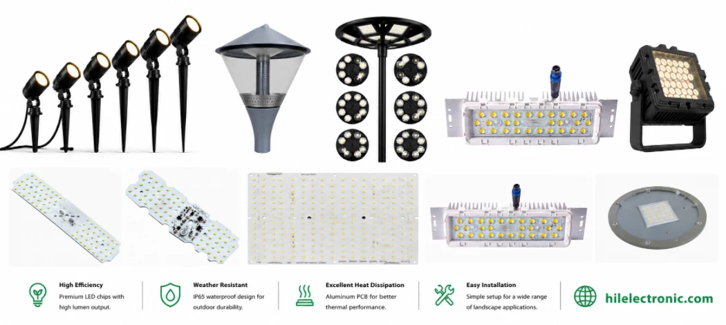
LED Landscape Light PCB Manufacturing — Uplight, Well Light & Underwater Engines
Figure 1. LED landscape light PCB production and assembly...
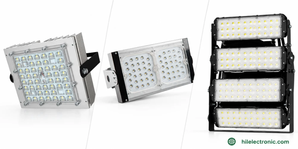
LED Parking Lot Light PCB Manufacturing & Assembly by Highleap Electronics
Figure 1. LED parking lot light PCB production and...
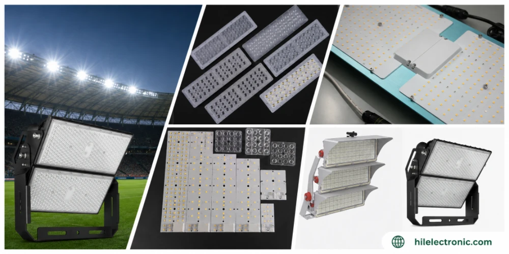
LED Stadium Light PCB Manufacturing — Very-High-Power Engines & Flicker-Free Drivers
Figure 1. LED stadium light PCB production and assembly...
How to get a quote for PCBs
Let‘s run DFM/DFA analysis for you and get back to you with a report. You can upload your files securely through our website. We require the following information in order to give you a quote:
-
- Gerber, ODB++, or .pcb, spec.
- BOM list if you require assembly
- Quantity
- Turn time
In addition to PCB manufacturing, we offer a comprehensive range of electronic services, including PCB design, PCBA, and turnkey solutions. Whether you need help with prototyping, design verification, component sourcing, or mass production, we provide end-to-end support to ensure your project’s success.
For PCBA services, please provide your BOM (Bill of Materials) and any specific assembly instructions. We also offer DFM/DFA analysis to optimize your designs for manufacturability and assembly, ensuring a smooth production process.