
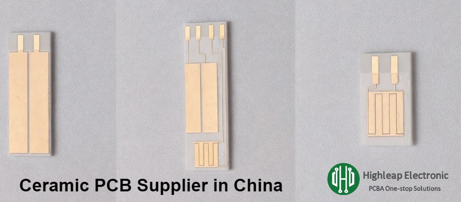
How to Choose a Ceramic PCB Supplier in China

Table of Contents
Sourcing a ceramic PCB supplier in China used to be a last resort — something you did only when domestic vendors quoted 3× the budget and 6-week lead times. Today, it is increasingly a first choice for engineering teams that need competitive pricing on alumina, aluminum nitride, or silicon nitride substrates without sacrificing process quality.
But the gap between a reliable ceramic PCB supplier and one that ships marginal boards is wider in China than in most Western markets, precisely because the range of factory capability is broader. This guide covers how to qualify, communicate with, and verify quality from a China-based ceramic PCB vendor — based on real procurement workflows, not theory.
1) Why More Engineers Are Sourcing Ceramic PCBs from China
1.1 Cost Structure Advantage
China’s electronics manufacturing ecosystem offers structural cost advantages for ceramic PCB production that go beyond labor rates:
- Raw material proximity: Major ceramic substrate suppliers (alumina, AlN) maintain production and distribution hubs in Guangdong, Jiangsu, and Zhejiang provinces, reducing material lead times and freight costs
- Shared infrastructure: Factories producing ceramic PCBs often share sintering, metallization, and laser drilling equipment across product lines, distributing capital costs more efficiently
- Integrated supply chains: A single facility can handle substrate preparation, metallization, circuit patterning, and PCB assembly services — eliminating cross-vendor markups
For projects using standard 96% alumina with thick-film metallization, China-sourced boards typically cost 30–50% less than equivalent boards from European or North American suppliers at comparable quality levels.
1.2 Capacity and Turnaround
China’s PCB manufacturing sector operates at a scale that enables fast turnaround even for specialized products. Many ceramic PCB factories maintain dedicated production lines that can process prototype orders in 7–10 business days and ramp to volume within 2–3 weeks — timelines that are difficult to match elsewhere.
2) Qualifying a Ceramic PCB Supplier in China: Step by Step
2.1 Initial Screening
Start by verifying basic capability before requesting quotes. A qualified ceramic circuit board manufacturer should demonstrate:
- ☐ Documented experience with your specific ceramic material (alumina, AlN, Si₃N₄)
- ☐ In-house metallization capability (DBC, thick film, or thin film — not outsourced)
- ☐ Relevant certifications (ISO 9001 at minimum; IATF 16949 for automotive; ISO 13485 for medical)
- ☐ English-speaking engineering contact who can discuss technical details directly
2.2 Sample Evaluation
Request evaluation samples before committing to production. Specify test criteria upfront:
| Parameter | What to Measure | Acceptable Tolerance |
|---|---|---|
| Substrate thickness | Micrometer measurement at 5 points | ±0.05 mm |
| Trace width / space | Optical inspection or cross-section | ±10% of nominal |
| Surface roughness (Ra) | Profilometer on bare ceramic | <0.8 µm (standard); <0.3 µm (thin film) |
| DBC peel strength | 90° peel test per IPC-TM-650 | >5 N/mm (acceptable); >8 N/mm (preferred) |
| Thermal shock survival | –40°C to +150°C cycling | >100 cycles without delamination |
For DBC-based projects, review our DBC ceramic substrate selection guide for material-specific quality benchmarks.
2.3 Factory Audit (Remote or On-Site)
If the project value justifies it, conduct a factory audit. Key areas to inspect:
- Ceramic substrate incoming inspection process and records
- Sintering furnace temperature uniformity data
- DBC bonding furnace atmosphere control documentation
- SPC records for critical dimensions across recent production lots
- Separation between ceramic and FR4 production lines (cross-contamination control)
Many China-based suppliers now offer video-guided virtual factory tours as an alternative to on-site visits.
3) Communication Protocols That Prevent Costly Mistakes
3.1 Specification Documents
Vague specifications are the single largest source of quality problems when working with overseas suppliers. Provide explicit documentation for every critical parameter:
- Material specification: State ceramic type, purity grade, and required thermal conductivity (e.g., “AlN, ≥170 W/m·K” — not just “aluminum nitride”)
- Dimensional drawing: Include tolerances on every dimension; do not assume the supplier will apply your preferred standard
- Surface finish: Specify finish type (ENIG, hard gold, Ni/Ag) and thickness range
- Acceptance criteria: Define pass/fail thresholds for each inspection parameter
3.2 DFM Review Process
A strong supplier performs ceramic PCB fabrication with DFM review before quoting. This means they analyze your design files and provide feedback on potential manufacturability issues — trace widths that are too narrow for the specified metallization method, via placements that risk ceramic cracking, or panelization layouts that reduce yield.
If a supplier accepts your files without any questions or feedback, that is a red flag — it suggests limited ceramic-specific process knowledge.
3.3 Language and Time Zone Management
Effective collaboration requires a bilingual engineering contact — not just a sales representative forwarding emails. Confirm that technical questions get answered by someone who understands ceramic PCB process parameters, not translated through a non-technical intermediary.
4) Quality Verification Before and After Shipment
4.1 In-Process Inspection Points
Request documentation from these critical checkpoints:
- After sintering: Substrate flatness and dimensional verification
- After metallization: Copper thickness, adhesion test results, trace width measurements
- After patterning: Electrical continuity and isolation testing
- After assembly (if applicable): SPI, AOI, and X-ray inspection results for SMT components
4.2 Final Inspection and Outgoing QC
Before shipment, require:
- ☐ Certificate of Conformance (CoC) with lot-specific test data
- ☐ Dimensional inspection report (sample size per AQL or 100% if critical)
- ☐ Reliability test data (thermal shock results, if specified in your PO)
- ☐ Photographs of finished boards (top, bottom, cross-section if DBC)
- ☐ Material traceability records linking boards to raw ceramic substrate lot numbers
4.3 Third-Party Verification
For high-value or safety-critical projects, consider engaging a third-party inspection service in China to verify outgoing quality before shipment. This adds 1–2 business days but can prevent receiving an entire lot of non-conforming boards.
5) Logistics, Lead Times, and IP Protection
5.1 Typical Lead Times from China
| Order Type | Fabrication Only | Fabrication + Assembly |
|---|---|---|
| Prototype (5–20 pcs) | 7–12 business days | 12–18 business days |
| Small batch (50–500 pcs) | 10–15 business days | 15–22 business days |
| Volume (1,000+ pcs) | 15–25 business days | 20–30 business days |
Add 3–5 business days for international shipping (express air freight) or 15–25 days for sea freight.
5.2 Intellectual Property Considerations
Protect your designs through:
- Non-Disclosure Agreements (NDAs) signed before sharing Gerber files
- Separating sensitive design elements across different suppliers when feasible
- Working with established manufacturers who hold international certifications — these companies have more to lose from IP violations and typically maintain stronger internal controls
6) Working with Highleap Electronics
Highleap Electronics operates from Guangzhou, China, providing integrated ceramic PCB fabrication and turnkey PCB assembly services under one facility. Our ceramic PCB capabilities include:
- Materials: Alumina (96% and 99.6%), aluminum nitride, silicon nitride
- Metallization: DBC and thick-film processing; thick film ceramic circuit board fabrication for hybrid and sensor applications
- Tolerances: Dimensional accuracy within ±0.05 mm; laser via capability down to 0.1 mm
- Assembly: Full SMT, wire bonding, die attach, conformal coating
- Quality system: ISO 9001, ISO 13485, ISO 14001, IATF 16949
- Communication: Bilingual engineering team with direct technical support
We provide free DFM review on all ceramic PCB projects and typically deliver quotes with engineering feedback within 48 hours. Our component sourcing services allow customers to consolidate fabrication, parts procurement, and assembly into a single purchase order — reducing logistics complexity and total lead time.
Contact our team with your Gerber files, BOM, and specifications to start the evaluation process.

Recommended Posts
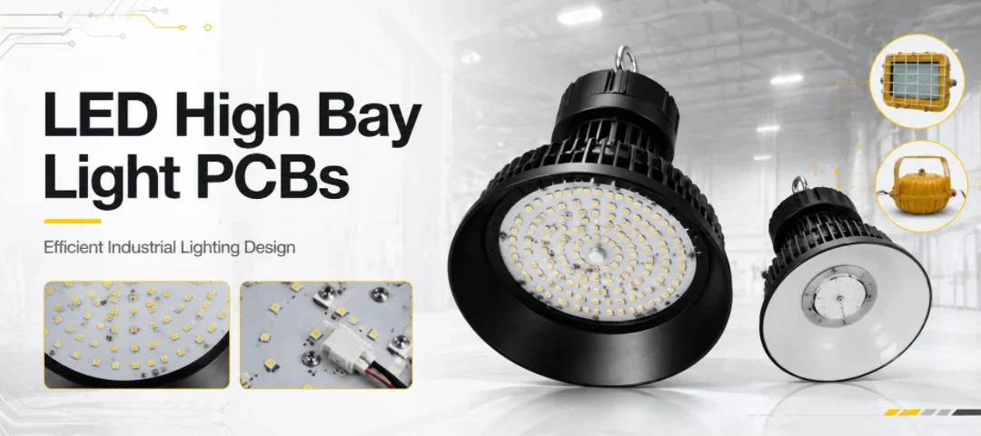
LED High Bay Light PCBs: Metal-Core Light Engines, Drivers & Turnkey Boards Built to Spec
Figure 1. LED high bay light PCB manufacturing reference....
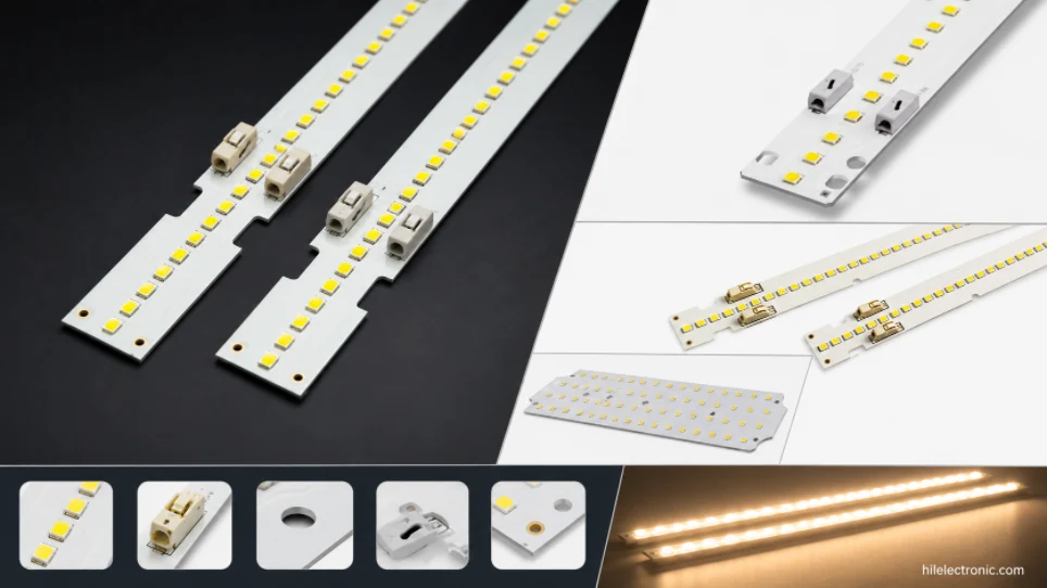
LED Linear & Strip Light PCBs: Long-Format Engines, Flexible & Rigid-Flex Boards
Figure 1. LED linear light PCB manufacturing reference....
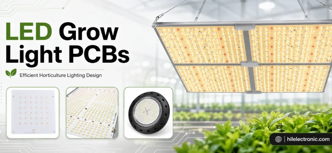
LED Grow Light PCBs: Multi-Channel Spectrum Boards, Drivers & Thermal Design
Figure 1. LED grow light PCB manufacturing reference....
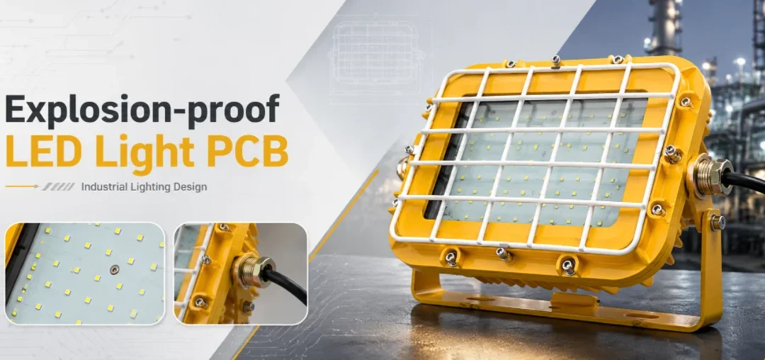
Explosion-Proof LED Light PCBs: Hazardous-Location Boards, Drivers & Assembly
Figure 1. explosion-proof LED light PCB manufacturing...
How to get a quote for PCBs
Let us run DFM/DFA analysis for you and get back to you with a report.
You can upload your files securely through our website.
We require the following information in order to give you a quote:
-
- Gerber, ODB++, or .pcb, spec.
- BOM list if you require assembly
- Quantity
- Turn time
In addition to PCB manufacturing, we offer a comprehensive range of electronic services, including PCB design, PCBA (Printed Circuit Board Assembly), and turnkey solutions. Whether you need help with prototyping, design verification, component sourcing, or mass production, we provide end-to-end support to ensure your project’s success. For PCBA services, please provide your BOM (Bill of Materials) and any specific assembly instructions. We also offer DFM/DFA analysis to optimize your designs for manufacturability and assembly, ensuring a smooth production process.