
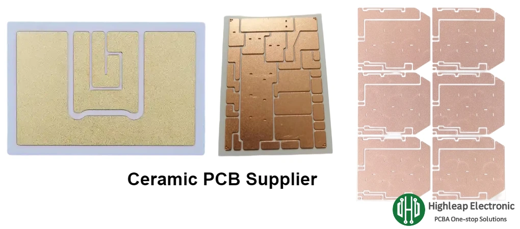
Ceramic PCB Supplier Evaluation for Electronics

Table of Contents
- Why Supplier Selection Matters More for Ceramic Than FR4
- Material Capability Assessment
- Process Control and Manufacturing Depth
- Certifications and Quality Systems
- Design-for-Manufacturability Support
- Assembly Integration and Turnkey Capability
- Supplier Evaluation Checklist and Red Flags
- Why Engineering Teams Choose Highleap Electronics
Finding a reliable ceramic PCB supplier is one of the most frustrating parts of developing high-power or high-frequency electronics. Unlike standard FR4 boards — where dozens of factories deliver acceptable quality at comparable prices — ceramic substrates require specialized equipment, material expertise, and process knowledge that fewer manufacturers genuinely possess.
Engineers often discover too late that their chosen vendor cannot hold the tolerances they need, cannot process the ceramic material they specified, or cannot scale from prototype to volume without quality drift. Every failed batch adds another re-qualification cycle and another month to an already tight development schedule.
This article provides a practical evaluation framework based on technical and operational capabilities — not marketing claims — so you can identify a ceramic PCB supplier that will actually deliver reliable boards on time.
1) Why Supplier Selection Matters More for Ceramic Than FR4
1.1 The Manufacturing Complexity Gap
FR4 PCB fabrication is a well-standardized process. Hundreds of manufacturers worldwide use essentially the same materials, equipment, and process flows. Switching between FR4 suppliers usually involves minimal risk.
Ceramic PCB fabrication is fundamentally different:
- Sintering temperatures exceed 1,500°C (vs. ~180°C lamination for FR4)
- Laser drilling parameters must be tuned per ceramic material (alumina vs. AlN vs. Si₃N₄)
- Metallization adhesion depends on surface preparation specific to each substrate
- CTE mismatch management requires process expertise that varies by bonding method (DBC vs. thick film vs. thin film)
The result: supplier capability varies enormously. Two factories both advertising “ceramic PCB” services may differ by an order of magnitude in yield, dimensional accuracy, and reliability performance.
1.2 The Cost of Getting It Wrong
Choosing the wrong ceramic circuit board vendor typically creates three compounding problems:
- Wasted prototype cycles: Boards that do not meet thermal or dimensional specs force redesign or re-sourcing
- Schedule delays: Re-qualification with a new supplier adds 4–8 weeks to the development timeline
- Hidden quality risks: Marginal suppliers may ship boards that pass initial inspection but fail under thermal cycling in the field
Investing time in proper supplier evaluation upfront avoids these downstream costs.
2) Material Capability Assessment
2.1 Which Ceramics Can They Actually Process?
The first filter is straightforward: does the supplier have documented production experience with the ceramic material your design requires? Many vendors advertise ceramic PCB capabilities but only handle alumina. If your application demands aluminum nitride or silicon nitride, you need a vendor whose production line is equipped and qualified for those specific materials.
A capable ceramic circuit board manufacturer should provide:
- Incoming inspection records for ceramic substrates (purity verification, dimensional checks, surface roughness)
- Process qualification reports per material type
- Documented experience with the specific purity grades you need (e.g., 96% vs. 99.6% alumina)
2.2 Material-Specific Questions to Ask
| If Your Design Uses… | Ask the Supplier… |
|---|---|
| Alumina (Al₂O₃) | Which purity grades do you stock? What is your standard surface roughness after lapping? |
| Aluminum Nitride (AlN) | What thermal conductivity do your AlN substrates achieve? Can you provide lot-level Tc data? |
| Silicon Nitride (Si₃N₄) | What is your fracture toughness specification? Do you have thermal cycling reliability data? |
| DBC substrates | What bonding furnace temperature accuracy do you maintain? What peel strength do you guarantee? |
For projects involving DBC bonding, review our DBC ceramic substrate material guide for detailed quality criteria before engaging a supplier.
3) Process Control and Manufacturing Depth
3.1 Key Process Indicators
A qualified supplier demonstrates manufacturing depth through:
- Process flow documentation: Clearly defined procedures for each ceramic material and metallization method
- SPC data: Statistical process control records for critical dimensions (trace width, via diameter, substrate thickness)
- Reliability test data: Thermal shock and power cycling results from production lots — not just from initial qualification samples
3.2 Understanding the Manufacturing Steps
The ceramic PCB manufacturing process involves specialized steps not found in conventional PCB production:
- Green tape preparation and via punching
- Screen printing of conductive and dielectric layers
- Lamination and co-firing (LTCC) or post-fire processing (HTCC)
- Sintering at temperatures exceeding 1,500°C
- Post-fire machining, laser trimming, and surface finishing
Each step introduces variability. Only suppliers with mature, documented process controls can maintain yield rates above 90% on complex multilayer ceramic designs.
3.3 Production Capability Benchmarks
| Capability | Acceptable | Preferred |
|---|---|---|
| Dimensional tolerance | ±0.10 mm | ±0.05 mm |
| Min. via diameter (laser) | 0.15 mm | 0.10 mm |
| DBC peel strength | >5 N/mm | >8 N/mm |
| Thermal shock survival | 100 cycles (–40/+125°C) | 500+ cycles (–40/+150°C) |
| Production lot yield | >85% | >93% |
4) Certifications and Quality Systems
4.1 Minimum Certification Requirements
Certifications alone do not guarantee quality, but their absence is a red flag. The certifications you should verify depend on your end market:
- General electronics: ISO 9001 (quality management system)
- Automotive: IATF 16949 (automotive quality management)
- Medical devices: ISO 13485 (medical device quality management)
- Environmental: ISO 14001 (environmental management)
- Aerospace/Defense: AS9100 or applicable MIL-spec compliance
4.2 Beyond the Certificate
Verify that the supplier applies these standards in daily practice — not just during audit season. Request recent audit reports, review their corrective action process (CAPA), and ask how they handle non-conforming material. Suppliers who welcome this scrutiny typically have the strongest quality systems.
5) Design-for-Manufacturability Support
5.1 Why DFM Matters More for Ceramic
The best ceramic PCB vendors do not just build what you send them — they help you avoid mistakes before fabrication begins. DFM review is particularly critical for ceramic substrates because the design rules differ significantly from standard PCBs:
- Minimum via sizes are larger than FR4 (typically 0.10–0.15 mm vs. 0.075 mm for FR4)
- Panelization constraints are stricter due to ceramic brittleness
- Certain pattern geometries that work on FR4 cause cracking or delamination on ceramic
- Thermal via placement must account for ceramic substrate integrity under thermal cycling
5.2 What to Expect from a Good Supplier
When evaluating a potential ceramic PCB fabrication partner, verify whether they:
- ☐ Provide free DFM/DFA analysis before quoting
- ☐ Offer material selection guidance based on your operating conditions
- ☐ Can run thermal management simulation to validate substrate and stackup choices
- ☐ Give specific feedback on pattern geometry, via placement, and panelization feasibility
- ☐ Have engineers accessible during your design phase — not just after you submit files
Suppliers who invest in these DFM capabilities save their customers significant time and money during the development cycle.
6) Assembly Integration and Turnkey Capability
6.1 The Handoff Problem
A common pain point is the gap between ceramic substrate fabrication and PCB assembly. Ceramic boards often require specialized assembly processes — high-temperature reflow profiles, wire bonding for die attachment, careful handling to avoid microcracking — that not every assembler is equipped to handle.
Working with a supplier that provides both fabrication and ceramic PCB assembly services under one roof eliminates the finger-pointing that happens when boards fail after assembly. When the same factory controls both processes, root cause analysis is faster and resolution more effective.
6.2 Capabilities to Verify
- ☐ High-temperature reflow profiling optimized for ceramic thermal characteristics
- ☐ Wire bonding (gold and aluminum) for hybrid circuit and die-attach applications
- ☐ Die attach with controlled bond line thickness and void content
- ☐ X-ray inspection for hidden joints (BGA, QFN, die attach)
- ☐ Conformal coating and encapsulation services
This is especially important for DBC substrate-based power modules, where the assembly process — die attach, wire bonding, encapsulation — must be carefully coordinated with the substrate metallization and dimensional tolerances.
6.3 The One-Vendor Advantage
| Factor | Split Supply Chain | Integrated Supplier |
|---|---|---|
| Failure root cause analysis | Vendor A blames Vendor B | One team, one investigation |
| Design iteration speed | Separate change orders, double lead time | Single ECO, coordinated response |
| Process optimization | Limited visibility between fab and assembly | Shared data, end-to-end optimization |
| Logistics complexity | Two shipping cycles, customs twice (if cross-border) | Single facility, one shipment |
7) Supplier Evaluation Checklist and Red Flags
7.1 Evaluation Checklist
Use this checklist when qualifying a new ceramic PCB supplier:
- ☐ Can process your required ceramic material (alumina, AlN, Si₃N₄, or BeO)
- ☐ Provides incoming substrate inspection data
- ☐ Has documented process flows and SPC records
- ☐ Holds relevant certifications for your end market
- ☐ Offers DFM review with actionable engineering feedback
- ☐ Can provide sample alumina boards or material-specific test coupons for evaluation
- ☐ Provides thermal shock and reliability test data from production lots
- ☐ Offers both fabrication and assembly under one roof (or has a qualified assembly partner)
- ☐ Maintains consistent lead times from prototype through volume
- ☐ Has a clear escalation path for engineering questions during production
7.2 Red Flags
Watch for these warning signs during your evaluation:
- No material-specific samples: Cannot provide test boards in your required ceramic material
- No DFM feedback: Accepts your files without comment — this suggests limited ceramic process knowledge
- Vague tolerances: Quoted specs are missing or use ambiguous language
- No in-house testing: Cannot test thermal resistance or dielectric breakdown on their production floor
- Mixed production lines: Ceramic and FR4 boards processed on the same equipment — cross-contamination risks adhesion failures
- Unstable lead times: Quoted 2 weeks but delivered in 5 — consistently
8) Why Engineering Teams Choose Highleap Electronics
At Highleap Electronics, we understand that selecting a ceramic PCB vendor is fundamentally an engineering decision, not just a procurement exercise. Our integrated capabilities address every evaluation criterion outlined above:
- Materials: We process alumina, aluminum nitride, and silicon nitride substrates with documented incoming inspection and lot traceability
- Metallization: DBC and thick-film processing with dimensional tolerances within ±0.05 mm
- Assembly: Full turnkey PCB assembly including SMT, wire bonding, die attach, and conformal coating
- Quality: ISO 9001, ISO 13485, ISO 14001, and IATF 16949 certified
- DFM: Free engineering review with material selection guidance and thermal optimization feedback
- Scale: From 10 prototype units to 10,000+ production boards with consistent process controls
Whether you are sourcing ceramic boards for power electronics, metal core PCBs for LED thermal management, or advanced substrates for RF and microwave applications, we bring the material expertise and process control to deliver boards that meet your specifications — not just on the first lot, but consistently across production volumes.
Contact our engineering team today with your Gerber files and specifications. We typically provide a detailed quote with DFM recommendations within 48 hours.

at Highleap Electronics
Helen supports international engineering teams with end-to-end PCB fabrication and assembly solutions, helping projects move from quick-turn prototypes to stable mass production. Her experience spans high-frequency and RF boards, complex multilayer stackups, rigid-flex, and flex PCB technologies across multiple industries.
By translating technical requirements into practical manufacturing plans, she helps customers improve manufacturability, reduce risk, and optimize cost and lead time—while maintaining consistent quality at scale.

Recommended Posts

TUC TU-872 SLK PCB for High-Speed FR-4 Cost Control
TUC TU-872 SLK occupies a commercially useful middle...

Shengyi S1000-2M PCB for Thick Multilayer Reliability
Shengyi S1000-2M is a high-Tg, low-CTE FR-4.0 laminate for...
Isola P25N PCB for No-Flow Bonding and Cavity Builds
Isola P25N is a polyimide UL HB No-Flo® specialty prepreg....
ITEQ IT-88GMW PCB for 77 GHz Radar Modules
A 76–81 GHz automotive radar PCB is an electromagnetic...
How to get a quote for PCBs
Let us run DFM/DFA analysis for you and get back to you with a report.
You can upload your files securely through our website.
We require the following information in order to give you a quote:
-
- Gerber, ODB++, or .pcb, spec.
- BOM list if you require assembly
- Quantity
- Turn time