
How to Specify Custom Ceramic PCB for Electronics

Table of Contents
If your power module, high-brightness LED array, or RF front-end is running into thermal limits on FR4, you are not alone. Standard laminate substrates top out around 0.3–0.5 W/m·K of thermal conductivity — orders of magnitude below what demanding applications require. A custom ceramic PCB bridges that gap, but only when the substrate material, metallization method, and dimensional specs are tailored to your actual operating conditions.
This guide covers the practical decisions engineers and procurement teams face when specifying a custom ceramic circuit board — from material trade-offs to quoting best practices — so you can move from concept to qualified hardware with fewer iterations.
1) Why Standard PCBs Fall Short in High-Power Applications
1.1 The Thermal Conductivity Gap
FR4 offers thermal conductivity of approximately 0.3 W/m·K. Even aluminum-core MCPCBs typically reach only 1–2 W/m·K through the dielectric layer. Compare that to ceramic substrates:
| Substrate Material | Thermal Conductivity (W/m·K) | Typical Use Cases |
|---|---|---|
| FR4 | 0.3–0.5 | General consumer electronics |
| Aluminum MCPCB | 1–2 (dielectric layer) | LED lighting, power supplies |
| Alumina (Al₂O₃ 96%) | 20–30 | Automotive sensors, standard LEDs |
| Aluminum Nitride (AlN) | 170–220 | High-power LEDs, IGBT modules, laser diodes |
| Silicon Nitride (Si₃N₄) | 70–90 | EV inverters, severe thermal cycling |
| Beryllium Oxide (BeO) | 250–300 | Aerospace, defense, RF/microwave |
When junction temperatures need to stay below target and external heat sinking alone is not enough, ceramic substrates become a design requirement rather than an upgrade.
1.2 When Custom Specifications Are Necessary
Catalog ceramic substrates work for evaluation. But production designs rarely match standard dimensions, copper patterns, or via layouts exactly. A custom-built ceramic circuit board lets you:
- Optimize substrate thickness for your specific thermal stack (thinner = lower Rth, but less mechanical rigidity)
- Match the coefficient of thermal expansion (CTE) precisely to your die-attach and solder materials
- Place thermal vias exactly where finite-element simulation identifies peak heat flux
- Define copper patterns for both electrical routing and heat spreading in one layout
This matters most in power electronics (IGBT modules, SiC/GaN converters) and in LED lighting systems where lumen maintenance and color stability depend directly on junction temperature control.
2) Ceramic Substrate Material Selection
2.1 Alumina (Al₂O₃)
Alumina is the most widely used ceramic PCB substrate. Available in 96% and 99.6% purity grades, it offers a practical balance of thermal performance, electrical insulation, and cost. 96% alumina suits most moderate-power applications; 99.6% provides lower surface roughness and tighter dielectric properties for thin-film circuits and high-reliability builds.
For a detailed breakdown of grades, fabrication methods, and application fit, see our alumina PCB manufacturing guide.
2.2 Aluminum Nitride (AlN)
AlN delivers 8–10× the thermal conductivity of alumina. It is the substrate of choice when heat densities exceed 100 W/cm² — common in high-power LED packages, laser diode sub-mounts, and power semiconductor modules. The trade-off is higher material and processing cost, plus more demanding metallization requirements.
2.3 Silicon Nitride (Si₃N₄)
Si₃N₄ provides the highest mechanical strength and fracture toughness among engineering ceramics. It is preferred for power modules that must survive severe thermal cycling — EV traction inverters, for instance, where substrates endure millions of swings between –40°C and 150°C. Its thermal conductivity (70–90 W/m·K) is lower than AlN but still far superior to FR4 or metal-core alternatives.
2.4 Beryllium Oxide (BeO)
BeO offers thermal conductivity up to 300 W/m·K — the highest of any ceramic substrate — but requires strict safety controls during machining and handling due to toxicity of beryllium dust. It is reserved for defense, aerospace, and specialized RF applications where no other material provides sufficient thermal performance. Explore our BeO ceramic circuit board page for detailed specifications and safety considerations.
2.5 Material Selection Decision Framework
- ☐ Is thermal conductivity above 30 W/m·K required? → Consider AlN or Si₃N₄ over alumina
- ☐ Will the board undergo >10,000 thermal cycles at ΔT > 100°C? → Prioritize Si₃N₄ for fracture toughness
- ☐ Is the application cost-sensitive with moderate thermal demands? → 96% alumina is likely sufficient
- ☐ Is operating frequency above 10 GHz? → Evaluate BeO or AlN for dielectric performance
- ☐ Is CTE match to silicon or SiC critical? → AlN (4.5 ppm/°C) or Si₃N₄ (2.6 ppm/°C) are closest to silicon (2.6 ppm/°C)
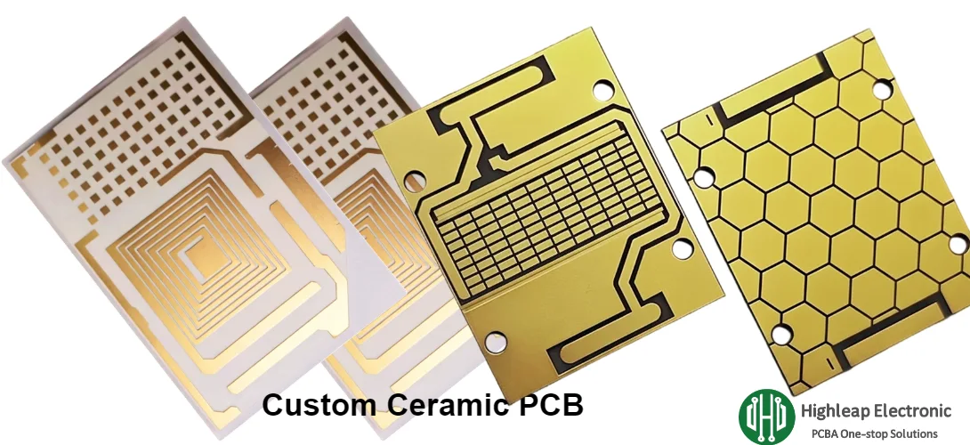
3) Metallization and Copper Bonding Methods
The way copper is bonded to a ceramic substrate directly impacts thermal resistance, current-carrying capacity, pattern resolution, and long-term reliability. Your application requirements determine the best metallization approach.
3.1 Direct Bonded Copper (DBC)
Copper foil is bonded directly to the ceramic at approximately 1,065°C through a controlled oxidation process, creating a metallurgical interface with extremely low thermal resistance. DBC supports thick copper layers (0.15–0.6 mm), enabling high-current power bus structures.
Best for: Power modules, IGBT substrates, EV inverters, and applications requiring >50A current paths. See our DBC substrate capabilities for process details and design guidelines.
3.2 Thick Film
Conductive pastes (silver-palladium, gold, or platinum) are screen-printed onto the ceramic and sintered at 850–1,000°C. Thick film offers design flexibility for embedded resistors and moderate-power circuits at lower cost than DBC.
Best for: Automotive sensors, industrial controls, hybrid circuits. See thick film ceramic PCB technology for trace specifications and substrate compatibility.
3.3 Thin Film
Metal layers are deposited by sputtering or evaporation, then patterned photolithographically. Thin film achieves the finest resolution (line/space down to 10 µm) and tightest dimensional tolerances.
Best for: RF/microwave circuits, high-frequency filters, precision analog applications where trace geometry controls impedance and insertion loss.
3.4 Metallization Comparison
| Method | Min. Line/Space | Cu Thickness | Typical Application |
|---|---|---|---|
| DBC | 0.3 mm / 0.3 mm | 0.15–0.6 mm | Power modules, high-current paths |
| Thick Film | 0.15 mm / 0.20 mm | 10–20 µm | Sensors, hybrid circuits |
| Thin Film | 0.01 mm / 0.01 mm | 0.1–5 µm | RF/microwave, precision analog |
4) Thermal Design Optimization for Custom Builds
4.1 Substrate Thickness Trade-offs
A custom ceramic printed circuit board is not just about material selection — it is about how the entire thermal stack works together. Substrate thickness is one of the most impactful variables:
- Reducing alumina from 0.635 mm to 0.38 mm cuts thermal resistance by approximately 40%
- Thinner substrates offer lower thermal impedance but reduce mechanical stiffness and handling robustness
- For power modules with base-plate mounting, substrate thickness must balance thermal performance against CTE-induced bending stress
Validate these trade-offs through simulation, then confirm with prototype testing. Our ceramic PCB thermal management guide covers simulation methodology and measurement techniques in detail.
4.2 Via Placement and Heat Spreading
Thermal vias filled with copper or silver paste provide low-resistance heat paths from component pads to the opposite side of the substrate. Effective via strategies include:
- Via arrays directly under high-power device thermal pads (15–25 vias/cm² for critical zones)
- Filled and capped vias to maintain planar surfaces for die attach or SMT
- Via diameter selection balancing thermal performance against ceramic substrate integrity (typically 0.2–0.3 mm for ceramic)
4.3 DFM Review and Thermal Consultation
Highleap Electronics provides DFM (Design for Manufacturability) review and thermal design consultation as part of our ceramic PCB fabrication service. Our engineering team helps you iterate between electrical and thermal constraints before committing to production tooling — avoiding costly re-spins.
5) What to Include in Your Custom Ceramic PCB Quote Request
Providing clear, complete specifications accelerates quoting and prevents engineering back-and-forth. When requesting a custom ceramic board quote, define the following:
5.1 Required Specifications
| Specification | Details to Provide |
|---|---|
| Ceramic material & purity | 96% Al₂O₃, 99.6% Al₂O₃, AlN, Si₃N₄, or BeO |
| Substrate dimensions & thickness | Panel/unit size, edge tolerances, cavity requirements |
| Metallization method | DBC, thick film, or thin film; copper thickness |
| Circuit pattern files | Gerber, ODB++; note any impedance-controlled traces |
| Surface finish | ENIG, hard gold (wire bonding), Ni/Ag (soldering) |
| Quantity & schedule | Prototype qty, production qty, target delivery date |
5.2 Assembly Specifications (If Applicable)
If you also need components mounted, provide your BOM and assembly drawings so we can quote ceramic PCB assembly services alongside fabrication. Include any special process notes: high-temperature reflow profiles, wire bonding requirements, or die-attach specifications.
5.3 Pre-Quote Checklist
- ☐ Ceramic material and purity grade selected
- ☐ Substrate dimensions, thickness, and tolerances defined
- ☐ Metallization method and copper thickness specified
- ☐ Gerber or circuit pattern files prepared
- ☐ Surface finish requirement identified
- ☐ Assembly requirements documented (BOM, placement, special processes)
- ☐ Quantity (prototype + production) and schedule noted
Get Your Custom Ceramic PCB Quote
6) From Prototype to Volume: Working with Highleap Electronics
6.1 Prototype Validation
Most custom ceramic PCB projects start with a small prototype run to validate thermal and electrical performance. Highleap supports this through our PCB prototyping services, which include rapid ceramic substrate fabrication, assembly of evaluation samples, and engineering feedback on design optimization.
6.2 Production Transition
Once prototypes pass validation, the transition to volume involves:
- Process qualification for yield consistency across production lots
- Incoming inspection criteria for raw ceramic substrates (purity, flatness, surface roughness)
- Automated assembly line setup for repeatable soldering, wire bonding, and encapsulation
Our ceramic circuit board manufacturing guide covers this transition in detail.
6.3 Why Engineers Choose Highleap
As a professional ceramic PCB manufacturer, Highleap Electronics brings substrate fabrication, metallization, and turnkey assembly under one roof:
- Materials: Alumina, aluminum nitride, and silicon nitride substrates
- Metallization: DBC and thick-film processing with ±0.05 mm dimensional tolerance
- Assembly: Full SMT, wire bonding, die attach, and conformal coating
- Certifications: ISO 9001, ISO 13485, ISO 14001, IATF 16949
- Scale: From 10 prototype units to 10,000+ production boards
One engineering team owns the entire process — your ceramic boards do not pass through three or four subcontractors before they reach your bench. When something needs adjustment, the feedback loop is immediate.
Ready to discuss your project? Send us your design files and specifications — our engineering team typically provides a detailed quote with DFM recommendations within 48 hours.

Recommended Posts

TUC TU-872 SLK PCB for High-Speed FR-4 Cost Control
TUC TU-872 SLK occupies a commercially useful middle...

Shengyi S1000-2M PCB for Thick Multilayer Reliability
Shengyi S1000-2M is a high-Tg, low-CTE FR-4.0 laminate for...
Isola P25N PCB for No-Flow Bonding and Cavity Builds
Isola P25N is a polyimide UL HB No-Flo® specialty prepreg....
ITEQ IT-88GMW PCB for 77 GHz Radar Modules
A 76–81 GHz automotive radar PCB is an electromagnetic...
How to get a quote for PCBs
Let us run DFM/DFA analysis for you and get back to you with a report.
You can upload your files securely through our website.
We require the following information in order to give you a quote:
-
- Gerber, ODB++, or .pcb, spec.
- BOM list if you require assembly
- Quantity
- Turn time
In addition to PCB manufacturing, we offer a comprehensive range of electronic services, including PCB design, PCBA (Printed Circuit Board Assembly), and turnkey solutions. Whether you need help with prototyping, design verification, component sourcing, or mass production, we provide end-to-end support to ensure your project’s success. For PCBA services, please provide your BOM (Bill of Materials) and any specific assembly instructions. We also offer DFM/DFA analysis to optimize your designs for manufacturability and assembly, ensuring a smooth production process.