
Isola I-Speed PCB Material for High Speed Circuits

As server architectures scale to support PCIe Gen 5 and telecommunications networks push beyond 400G Ethernet, hardware engineers face a strict signal integrity budget. Standard FR-4 laminates introduce unacceptable insertion loss, causing digital eye diagrams to collapse over long routing channels. To preserve signal clarity without absorbing the extreme costs of PTFE (Teflon) materials, the industry standard solution is Isola I-Speed.
However, selecting the right high-speed digital laminate is only half the battle. The true challenge lies in factory execution. High-layer-count server backplanes require flawless mechanical registration, precise impedance control, and advanced via drilling techniques to prevent internal short circuits. As a specialized China Isola I-Speed PCB manufacturer, Highleap Electronics has engineered this technical guide to help you understand the material’s properties, the true drivers of manufacturing cost, and how to successfully transition your high-speed design into mass production.
Request an Isola I-Speed Fabrication Quote
Table of Contents
Isola I-Speed Datasheet: Core Material Properties
When engineers evaluate a custom Isola I-Speed high speed PCB, they are looking for a substrate that bridges the gap between traditional epoxy and expensive RF laminates. Isola I-Speed utilizes a proprietary low-loss resin system combined with advanced glass styles (such as spread glass) to minimize the “fiber weave effect” and reduce timing skew in differential pairs.
The critical datasheet parameters that dictate signal integrity include:
- Dielectric Constant (Dk): A stable 3.30 (at 10 GHz). This lower Dk allows signals to propagate faster and reduces the capacitive load on high-speed traces.
- Dissipation Factor (Df): An ultra-low 0.0071 (at 10 GHz). This significantly reduces signal attenuation (insertion loss) across long backplane routing channels.
- Thermal Robustness: With a Glass Transition Temperature (Tg) of 180°C and a Decomposition Temperature (Td) of 360°C, the Isola I-Speed circuit board withstands multiple lead-free SMT reflow cycles and high operating temperatures in dense server racks without delamination.
Manufacturing Cost Drivers in I-Speed Multilayer Board Fabrication
For procurement teams, the most attractive feature of Isola I-Speed is not just its electrical performance, but its FR-4 processability. Unlike PTFE (Teflon) high-frequency boards that require hazardous sodium etching or expensive vacuum plasma desmear cycles, I-Speed can be desmeared and plated using standard alkaline permanganate chemistry lines.
The Hybrid Stackup Advantage
To drastically optimize your Isola I-Speed PCB fabrication quote, experienced designers rarely use this advanced material for every layer of a 24-layer server board. Instead, they design hybrid stackups.
- Because I-Speed’s resin system shares compatible curing kinetics and pressing temperatures with standard high-Tg FR-4 (like Isola 370HR), they can be co-cured in the same lamination press cycle.
- We routinely place I-Speed on the critical outer and specific internal layers for PCIe Gen 5 routing, while using low-cost 370HR for power, ground, and slow digital logic layers. This slashes material costs while maintaining a perfectly flat panel free from asymmetric warpage.
Preventing CAF Failure in High-Density Backplanes
As telecommunications equipment shrinks, via pitch (the distance between drilled holes) becomes incredibly tight. In high-layer-count server boards operating under continuous voltage bias, the greatest reliability threat is Conductive Anodic Filament (CAF) failure. CAF occurs when copper ions migrate along the glass fiber bundles between two closely spaced vias, causing an invisible, internal short circuit.
The Machining Bottleneck
While the I-Speed resin is chemically formulated to be highly CAF resistant, improper factory machining can destroy this protection. If an inexperienced Isola I-Speed server PCB factory utilizes dull drill bits or incorrect plunge speeds (chip load) during I-Speed multilayer board fabrication, the blunt mechanical trauma will fracture the glass fibers surrounding the via wall. These microscopic fractures create hollow capillary channels for copper ions to travel through.
The Highleap Manufacturing Solution
To ensure absolute CAF reliability, we enforce strict mechanical drilling protocols. We drastically reduce the “hit count” limit for our CNC drill bits—discarding them far earlier than standard FR-4 limits to guarantee a razor-sharp cut. By optimizing spindle RPMs and utilizing step-drilling techniques for high aspect ratios, we cleanly shear the advanced glass styles rather than tearing them, maintaining the integrity of the dielectric barrier.
DFM Guideline: Impedance and Laser Direct Imaging (LDI)
To hit tight ±5% impedance tolerances on 100-ohm differential pairs, the physical trace geometry must be perfect. Any over-etching creates a trapezoidal trace that causes signal reflection. We mandate the use of Laser Direct Imaging (LDI) and vacuum etching lines for all high-speed digital routing, ensuring perfectly vertical trace sidewalls.
Trace Tolerances for a Quick Turn Isola I-Speed PCB Prototype
Time-to-market is the primary driver in the telecom industry. When requesting a quick turn Isola I-Speed PCB prototype to validate your Signal Integrity (SI) simulations, it is vital to supply complete stackup and impedance requirements upfront.
Before launching fabrication, our CAM engineers will perform a rigorous Design for Manufacturability (DFM) check. We utilize advanced impedance calculators (like Polar Instruments) to cross-reference your trace widths and dielectric spacing against our physical etching capabilities. If adjustments are required to hit your 50-ohm single-ended or 100-ohm differential targets, we provide a modified stackup report for your approval prior to production.
Turnkey SMT Assembly for High-Speed Telecom Boards
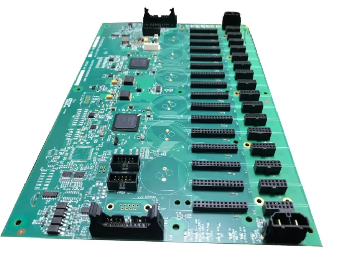
A high-speed digital backplane is incredibly complex, often featuring heavy copper planes, thousands of BGA pads, and massive thermal mass. Trusting the bare board fabrication to one vendor and the component assembly to a third party introduces significant thermal profiling risks during the soldering phase.
Working with a dedicated Isola I-Speed backplane PCB supplier and Isola high speed PCB maker eliminates logistical blind spots. We seamlessly transition your project from our advanced high-speed bare board lines directly into our precision PCBA manufacturing facility.
To guarantee that thick, heavy server boards absorb heat evenly during SMT reflow without warping, our process engineers develop highly customized thermal profiles. By utilizing 3D Automated Optical Inspection (AOI) and X-Ray (AXI) technology, we verify every hidden BGA solder joint, ensuring your 400G switches and data center routers operate flawlessly in the field. Explore our extensive PCB laminate material selection or contact our engineering team today to launch your high-speed project.

Recommended Posts
LED Parking Lot Light PCB Manufacturing & Assembly by Highleap Electronics
Figure 1. LED parking lot light PCB production and...
LED Stadium Light PCB Manufacturing — Very-High-Power Engines & Flicker-Free Drivers
Figure 1. LED stadium light PCB production and assembly...
LED Tunnel Light PCB Manufacturing — High-Reliability Engines & Drivers
Figure 1. LED tunnel light PCB production and assembly...
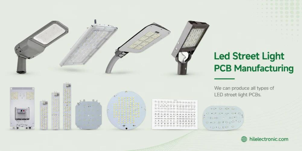
LED Street Light PCB Manufacturing & Assembly by Highleap Electronics
Figure 1. LED street light PCB production and assembly...
How to get a quote for PCBs
Let us run DFM/DFA analysis for you and get back to you with a report.
You can upload your files securely through our website.
We require the following information in order to give you a quote:
-
- Gerber, ODB++, or .pcb, spec.
- BOM list if you require assembly
- Quantity
- Turn time