
Blind Via PCB Price Per Board and HDI Cost Analysis

Table of Contents
- What Determines Blind Via PCB Price: The Cost Structure Breakdown
- Laser Drilling vs. Mechanical Drilling: Cost Structure and Selection Logic
- How Via Count, Geometry, and Fill Specification Drive Price
- Volume Pricing, NRE Amortization, and Repeat Order Economics
- Design-Stage Cost Reduction: Seven Techniques That Don’t Compromise Performance
- Hidden Costs That Inflate Blind Via PCB Quotes
- Blind Via PCB Fabrication at Highleap Electronics
Blind via PCBs are priced differently from standard through-hole boards because process complexity — not material — is the primary cost driver. Three variables account for 50–65% of total unit cost: drilling method (laser vs. mechanical), lamination cycle count (which determines HDI type), and via fill specification (unfilled vs. resin plug vs. copper-filled). A Type III HDI board with copper-filled stacked microvias on a 100×100 mm footprint routinely costs 5–6× more than a standard 6-layer board of identical size, not because the material is 5× more expensive, but because it requires four to six sequential lamination cycles, dedicated laser drilling programs, and X-ray inspection at every stage. Conversely, a Type I HDI design with mechanical-drilled 0.20 mm unfilled blind vias on the outer layers adds only 30–40% to the cost of a standard equivalent. The cost range between these two outcomes is not a supplier pricing variable — it is an engineering variable, and it is fully controllable at the design stage.
Get Transparent Blind Via PCB Pricing
1. What Determines Blind Via PCB Price: The Cost Structure Breakdown
On a standard through-hole PCB, cost is driven primarily by board area, layer count, and material. On a blind via HDI board, process complexity overtakes material as the primary cost driver. The cost structure breaks down as follows.
Drilling (25–40% of total cost). Laser drilling setup runs $80–$250 per panel regardless of via count, plus $0.008–$0.025 per via. Mechanical drilling setup costs $15–$50 per panel with per-hole costs of $0.002–$0.008. For high microvia density boards, drilling alone can represent 35% or more of unit cost.
Lamination cycles (15–25% of total cost). Each additional lamination cycle adds press time, registration steps, material cost, and yield risk. Type I HDI requires two lamination cycles. Type III HDI with buried vias requires four to six. Every additional cycle multiplies the opportunity for registration error and delamination — which is why Type III boards cost 5–6× a standard PCB of identical size.
X-ray inspection and electrical testing (8–15% of total cost). Blind via integrity cannot be verified visually or by standard AOI. X-ray inspection adds $3–$12 per panel at sampling rates, or $8–$15 per panel for 100% inspection. Flying probe electrical test adds $3–$8 per panel. For low-volume or Class 3 production, testing cost per board is significant.
Materials, imaging, plating, and outer processing (remaining 35–45%). These cost elements behave similarly to standard PCB pricing. Base material typically represents 15–25% of total cost — a smaller share than on standard boards — which confirms that process complexity, not material, is the controlling variable for blind via pricing.
1.1 HDI Type Classification and Price Multiples
The following comparison uses a controlled example: 100×100 mm board, 6 layers, 1.6 mm thickness, ENIG surface finish, 100-piece quantity, standard FR4. Price multiples are driven almost entirely by lamination cycles and drilling cost. For a detailed breakdown of each HDI stackup type and its manufacturing implications, refer to the HDI stack-up guide.
| HDI Configuration | Via Structure | Lamination Cycles | Price per Board (100 pcs) | Price Multiple |
|---|---|---|---|---|
| Standard 6-layer through-hole | All vias penetrate full stackup | 1 | $12–$18 | 1.0× |
| Type I HDI (1+4+1) | Blind L1–L2, L6–L5; through-holes L1–L6 | 2 | $28–$42 | 2.3–2.8× |
| Type II HDI (1+2+2+1) | Blind L1–L2, L1–L3, L6–L5, L6–L4; no through-holes | 3 | $48–$72 | 4.0–5.0× |
| Type III HDI with buried vias | Buried L3–L4, blind L1–L2, L6–L5, through-holes | 4–6 | $65–$95 | 5.4–6.5× |
1.2 Per-Via Cost Reference
Via fill specification has a larger cost impact than via diameter or drilling method. A copper-filled and planarized via costs 10–30× more per via than the same via left unfilled. Fill should only be specified where structurally required — via-in-pad locations under BGA and QFN pads, and stacked microvia structures where the next buildup layer drills directly on top.
| Via Type | Diameter | Fill Specification | Cost per Via |
|---|---|---|---|
| Laser-drilled microvia | 0.10 mm | Unfilled | $0.015–$0.035 |
| Laser-drilled microvia | 0.15 mm | Unfilled | $0.012–$0.025 |
| Mechanical blind via | 0.20 mm | Unfilled | $0.008–$0.018 |
| Mechanical blind via | 0.30 mm | Unfilled | $0.005–$0.012 |
| Any blind via | Any | Resin plug fill | Add $0.05–$0.15 |
| Any blind via | Any | Copper fill + planarization | Add $0.20–$0.60 |
A typical smartphone HDI board with 800 laser-drilled 0.10 mm microvias, left unfilled, carries $12–$28 in via drilling cost before lamination, materials, or any other processing. Adding copper fill and planarization to those same 800 vias adds $160–$480 per board — often exceeding the base fabrication cost.
2. Laser Drilling vs. Mechanical Drilling: Cost Structure and Selection Logic
The choice between laser and mechanical drilling is determined first by via diameter. For finished diameters below 0.20 mm, mechanical drilling is not reliably achievable and laser drilling is the only viable method. For diameters at or above 0.20 mm with aspect ratios at or below 5:1, mechanical drilling is available and significantly cheaper. Understanding where each method applies is essential to evaluating whether a quote is correctly specified.
2.1 Laser Drilling Cost Structure
CO₂ and UV laser drilling is the standard method for microvias ≤0.15 mm diameter. Its cost has two components that behave differently at different volumes.
Setup cost: $80–$250 per panel, regardless of via count. At low via counts, setup cost dominates — a panel with 50 vias carries $1.60–$5.00 in setup cost per via. A panel with 2,000 vias carries only $0.04–$0.13 per via from setup alone.
Per-via processing cost: $0.008–$0.025 per via, depending on laminate type, copper foil weight, via diameter, and the number of laser pulses required to penetrate each layer. Harder laminates such as high-Tg and ceramic-filled materials require more pulses and cost more per via.
Capacity constraint cost. Laser drilling is time-limited, not hole-count limited. A panel with 2,000 vias may require 30–60 minutes of dedicated laser time. During peak production periods, capacity bottlenecks result in 15–30% surcharges when lead time is compressed.
2.2 Mechanical Drilling Cost Structure
Mechanical controlled-depth drilling applies for blind vias ≥0.20 mm finished diameter and aspect ratios ≤5:1. On a standard 1.6 mm board, this limits mechanical blind vias to approximately 0.8 mm depth — reaching from L1 into L4 or L5 in a six-layer stackup, but not deeper.
Setup cost: $15–$50 per panel, significantly lower than laser because standard CNC programming is used without optical calibration.
Per-via cost: $0.002–$0.008 per via. Mechanical drilling is 2–4× cheaper per via than laser drilling for equivalent diameters in the eligible range.
Tool wear. Drill bits require replacement after 2,000–8,000 hits depending on laminate hardness. For hard materials at high via counts, tool amortization adds measurable per-via cost that manufacturers factor into pricing.
2.3 Hybrid Drilling: Applying Both Methods to One Design
Most HDI designs contain fine-pitch signal vias that require laser drilling alongside larger power and thermal vias that do not. Specifying mechanical drilling for every eligible via — diameter ≥0.20 mm, aspect ratio ≤5:1 — and laser drilling only where required reduces cost without any design change.
Worked example: An 8-layer Type II HDI board has 400 signal vias at 0.15 mm diameter (laser-required) and 150 power vias at 0.30 mm diameter (mechanical-eligible).
Pure laser cost: 550 × $0.020 = $11.00/board.
Hybrid cost: (400 × $0.020) + (150 × $0.006) = $8.90/board.
Saving: $2.10/board (19%). At 500 boards: $1,050 saved.
2.4 When Laser Drilling Is Non-Negotiable
The laser drilling cost premium is unavoidable in four conditions:
- Via diameter below 0.20 mm. Mechanical drills cannot reliably produce consistent hole geometry or copper plating below this threshold.
- Via-in-pad on fine-pitch BGAs. 0.40 mm pitch BGAs require 0.15 mm vias landing inside a 0.25 mm pad. The positional accuracy requirement (±0.025 mm or better) is only achievable with laser drilling on fiducial-registered panels.
- Stacked microvia structures. Laser-drilled microvias have a 1:1 aspect ratio (depth equals diameter), enabling shallow layer-to-layer transitions that can be stacked across buildup layers. Mechanical drilling cannot achieve the geometry required for reliable stacked configurations.
- Via densities above 500 per square inch. At these densities, mechanical drilling causes panel flexing and cumulative registration drift that makes positional accuracy unacceptable.

3. How Via Count, Geometry, and Fill Specification Drive Price
3.1 Via Density and Manufacturer Pricing Tiers
Via density affects pricing in two ways: directly through drilling time, and indirectly through the inspection and registration requirements it triggers. Most manufacturers apply density-based price adjustments above threshold levels.
| Via Density | Range | Typical Price Adjustment | Process Trigger |
|---|---|---|---|
| Low | <50 vias per 100 cm² | Baseline | Standard drilling and inspection |
| Medium | 50–200 per 100 cm² | +5% to +15% | Fiducial-based panel registration required |
| High | 200–500 per 100 cm² | +15% to +35% | X-ray drill registration; tighter lamination tolerances |
| Ultra-high | >500 per 100 cm² | +35% to +60% | Advanced laser systems; 100% X-ray inspection required |
3.2 Stacked vs. Staggered Microvias: The Fill Cost Decision
The choice between stacked and staggered microvias is one of the highest-leverage cost decisions in HDI via design. Stacked microvias are drilled through multiple consecutive buildup layers at the same X-Y position. They enable the highest routing density but require each via to be filled and planarized before the next buildup layer can be laminated and drilled. The cost impact is substantial: resin fill between lamination stages adds $0.05–$0.15 per via; planarization adds $1.50–$5.00 per panel; and first-run scrap rates increase by 3–8% due to fill quality failures that are only detectable after the second drilling operation.
Staggered microvias — offset by a minimum of 0.25 mm between layers — eliminate the fill requirement entirely. Staggering requires slightly more routing area for the offset pad capture zones but avoids fill cost, planarization cost, and the associated scrap risk entirely. For designs that also use buried vias in inner layers, each buried via layer pair introduces an additional core drilling and plating cycle, adding further lamination cost that compounds with blind via complexity.
Worked example: A board with 200 stacked vias across three buildup layers.
Stacked with fill: 200 × $0.10 = $20/board additional.
Staggered without fill: $0 additional.
At 100 boards: $2,000 saved with no change to electrical performance, only to routing geometry.
3.3 Panel Utilization and Via Distribution
Laser drilling operates on the full panel, not on individual boards. A board with all blind vias concentrated in a BGA corner forces the laser to process that region at high intensity while the rest of the panel is sparsely used — reducing efficiency without reducing time or cost. Distributing vias more uniformly across board area, where routing permits, can improve panel drilling efficiency by 10–20%. For multi-board panels, rotating alternating boards 180° balances via density across the panel and achieves a comparable efficiency gain.
4. Volume Pricing, NRE Amortization, and Repeat Order Economics
4.1 How Volume Reduces Unit Price
The per-unit price curve for blind via HDI boards is steep at low quantities and flattens significantly above 500 pieces. The steepest reduction — 60–70% — occurs between 5 and 100 pieces, driven almost entirely by NRE amortization and panel utilization improvement. From 100 to 2,000 pieces, further reductions of 30–40% come from material volume pricing and optimized press loading. Beyond 2,000 pieces, the marginal reduction drops to 5–15%.
| Quantity | Unit Price — Type I HDI | Unit Price — Type II HDI | Primary Cost Driver at This Volume |
|---|---|---|---|
| 5 pcs (prototype) | $60–$90 | $110–$160 | Full NRE loaded; minimum panel charge |
| 25 pcs | $38–$55 | $72–$105 | NRE begins amortizing across more boards |
| 100 pcs | $28–$42 | $52–$75 | Full panel utilization; NRE below $12/board |
| 500 pcs | $22–$32 | $42–$58 | Material volume pricing; NRE below $2.30/board |
| 2,000 pcs | $18–$25 | $35–$48 | Bulk procurement; dedicated tooling; yield improvement |
4.2 NRE Cost and Its Per-Board Impact
Non-recurring engineering charges for blind via HDI boards include stackup engineering and impedance modeling ($150–$500), laser drilling program generation ($100–$300), photo-tooling for all layers ($80–$200), and test fixture fabrication ($50–$150). Total NRE typically runs $380–$1,150 depending on board complexity. When requesting a blind via PCB quote, specifying the exact HDI type and via interconnection scheme is essential — without this information, manufacturers cannot allocate NRE or drilling costs accurately, and vague requests often result in quotes with large contingency buffers.
The per-board NRE contribution explains why prototype pricing appears disproportionately high. At 5 pieces, NRE adds $76–$230 per board. At 100 pieces, it adds $3.80–$11.50 per board. At 500 pieces, it adds $0.76–$2.30 per board. Material and processing costs are essentially identical at prototype and production quantities — the 3–4× price multiple between a 5-piece and a 500-piece run is almost entirely explained by NRE allocation, not by any difference in manufacturing cost per unit.
4.3 Repeat Order Pricing and Tooling Retention
Once NRE is paid on the first order, repeat orders within the manufacturer’s tooling retention window — typically 12–24 months — eliminate NRE charges entirely. This creates a significant and often underutilized price advantage on follow-on small-batch production.
Example: First order of 100 boards: $38/board ($3,800 total, NRE included). Repeat order of 100 boards six months later: $26/board ($2,600 total, tooling reused). That is a 32% unit cost reduction on the repeat order — same board, same manufacturer, no process changes. For products with recurring production schedules, always confirm the tooling retention period upfront and whether repeat order pricing is applied automatically.

5. Design-Stage Cost Reduction: Seven Techniques That Don’t Compromise Performance
The most effective cost reduction for blind via PCBs happens in CAD, not in negotiation. Each of the following design decisions reduces manufacturing cost while preserving electrical and mechanical performance.
5.1 Increase Via Diameter to the Mechanical Drilling Threshold Where Possible
If a design specifies 0.15 mm blind vias throughout but only vias under fine-pitch BGA pads (0.40 mm pitch or tighter) actually require that diameter, increase all other vias to 0.20 mm. At 0.20 mm, mechanical drilling becomes available and reduces per-via cost by 50–65% on those vias. Converting 200 vias from laser to mechanical saves $2.40/board. At 500 boards, that is $1,200.
5.2 Remove Fill Specifications from Vias That Don’t Require Them
Via filling is electrically and mechanically necessary only at via-in-pad locations and in stacked microvia structures. All other blind vias can be left unfilled without affecting signal integrity, power delivery, or reliability. Audit your fabrication notes: if vias are specified as filled but are neither in-pad nor stacked, remove the fill requirement. Eliminating fill on 200 non-critical vias at $0.10/via saves $20/board, or $10,000 at 500 boards.
5.3 Convert Stacked Microvias to Staggered Where Layout Allows
Stacked microvias require fill and planarization between lamination stages. Staggered microvias — offset ≥0.25 mm — achieve the same layer-to-layer interconnection without fill. Review the stackup for stacked via structures that are not constrained by escape routing density. Converting them to staggered eliminates per-via fill cost plus planarization panel charges with no signal path change.
5.4 Evaluate Whether Type I HDI Can Replace Type II
The step from Type I HDI to Type II adds one lamination cycle and typically increases unit price by 60–80%. If connections currently routed through L1–L3 vias can be reassigned to L1–L2 vias with adjusted signal layer assignments, the design may be manufacturable as Type I. A 30–50% unit cost reduction is achievable from this single change, particularly valuable at volumes below 500 pieces.
5.5 Reduce Layer Count Through HDI Via Strategy
Blind vias recover routing channels that through-holes consume across all layers. A board initially designed as a standard 8-layer PCB may be achievable as 6-layer Type I HDI with equivalent routing capacity. Base material and lamination cost for a 6-layer board is 25–35% less than an 8-layer board. If the HDI conversion also allows a smaller board footprint, the material saving compounds further, and the net cost of the HDI approach can be lower than the through-hole baseline despite carrying a via complexity premium.
5.6 Use Asymmetric Tolerances to Reduce Inspection Requirements
Specifying finished via diameter as 0.20 mm ±0.02 mm requires equal control in both directions. Specifying 0.20 mm +0.03/−0.02 mm imposes the same minimum size floor for reliability but allows more over-drilling tolerance, reducing process control stringency and associated cost. Similarly, relaxing layer-to-layer registration from ±0.075 mm to ±0.10 mm — where your minimum via-to-trace clearance of 0.15 mm provides sufficient margin — reduces X-ray alignment requirements and drilling cost by 5–12%.
5.7 Prototype with a Simplified Via Structure Before Committing to Production Tooling
For prototype PCB runs of 5–25 pieces, build a simplified version of the target design to validate functionality before committing to the full via structure. Prototype with only L1–L2 blind vias even if production requires L1–L3; route L1–L3 connections through L2 as a functional approximation. Prototype with staggered vias if production uses stacked. Use mechanical drilling for all vias ≥0.20 mm to eliminate laser setup charges. These simplifications reduce prototype cost by 30–50% while providing the functional validation needed to commit production tooling to the full design.
6. Hidden Costs That Inflate Blind Via PCB Quotes
6.1 Yield Loss Allocation
Blind via HDI boards have lower first-pass yield than standard PCBs. The three primary failure modes are blind via opens (incomplete copper plating in the barrel, occurring at 2–5% of vias on first production runs and below 1% once process capability is established), registration errors (blind via drilled partially off-pad due to layer misalignment, affecting 1–3% of boards during initial setup), and delamination at buildup layer interfaces (below 1% on most designs but increasing with lamination cycle count and board thickness).
Manufacturers price yield loss into quotes by fabricating 3–8% more boards than ordered, with the excess covering expected scrap. This adds 3–8% to effective unit cost on new designs. On repeat orders where process capability (Cpk) is established, the yield allocation drops below 2%. Ask whether yield loss is factored into first-article quotes and whether pricing adjusts on repeat orders as the manufacturer’s process matures on your specific design.
6.2 Testing Costs by Inspection Level
| Test Method | Cost per Panel | Applicable When |
|---|---|---|
| Visual inspection | $0.50–$1.50 | All orders (standard) |
| Flying probe electrical test | $3.00–$8.00 | Standard for production orders |
| X-ray inspection (5 boards per lot) | $2.00–$5.00 | IPC Class 2 blind via verification |
| X-ray inspection (100% of boards) | $8.00–$15.00 | IPC Class 3, medical, aerospace |
| Micro-section analysis (destructive) | $50–$150 per sample | First article and process qualification |
| TDR impedance coupon testing | $5.00–$12.00 | When controlled impedance is specified |
On a 10-board prototype panel, Class 3 testing — 100% X-ray, electrical test, and impedance coupon — adds $16–$35 per panel, or $1.60–$3.50 per board. At 100 boards across 10 panels, total testing cost reaches $160–$350. When comparing quotes, verify that testing scope is specified identically across all suppliers. A lower unit price that omits X-ray inspection on a Class 2 design is not a comparable quote.
6.3 Expedite Premiums
Standard lead time for Type I HDI is 10–15 business days; Type II requires 15–20 days. Expedite pricing applies as follows: 7-day turnaround adds 25–40%; 5-day turnaround adds 40–60%; 3-day super rush for Type I only adds 80–120%. Type II and Type III require multiple lamination cycles and are not achievable in 3 days at most facilities.
On a $3,000 base order, a 5-day expedite adds $1,200–$1,800. Confirming production schedules 4–6 weeks in advance eliminates this cost entirely for recurring production.
6.4 Specialty Laminate Surcharges
Standard FR4 is commodity-priced and forms the baseline. Specialty laminate premiums over standard FR4: High-Tg FR4 (Tg ≥170°C) adds 15–30%; halogen-free FR4 adds 20–40%; mid-loss laminates such as Megtron 6 add 200–400%; low-loss RF laminates such as Rogers RO4000 series add 400–1,000%.
For HDI boards where RF or high-speed signal performance requires low-loss material only on the outer signal layers, a hybrid stackup — Rogers or Megtron 6 on L1 and L6, standard FR4 on inner layers — cuts material cost 40–60% compared to a full-laminate premium build while preserving the electrical performance on the layers that carry critical signals.
7. Blind Via PCB & Advanced PCB Manufacturing at Highleap Electronics
Highleap Electronics fabricates blind via HDI boards from Type I through Type III, including stacked microvia structures, buried via combinations, and hybrid stackups with Rogers or Megtron outer layers on FR4 inner cores. Capabilities extend beyond blind via boards to the full range of advanced PCB types — multilayer standard boards, rigid-flex, high-frequency RF, heavy copper, and metal core — allowing engineering teams to consolidate all board types within a single supply chain.
All blind via fabrication is quoted with full line-item transparency: drilling method and setup, lamination cycles, via fill specification, testing level, and NRE are itemized separately. Every quote includes a complimentary DFM review covering via diameter eligibility for mechanical versus laser drilling, fill specification necessity, stacked-to-staggered conversion opportunities, HDI type reduction analysis, and panel utilization assessment — typically identifying 10–30% cost reductions without design re-spin. Tooling is retained for 24 months, with repeat orders within that window priced without NRE.
For projects requiring board-level assembly following fabrication, SMT PCB assembly is available in-house with seamless transfer from the bare board line — eliminating the logistics risk of moving sensitive HDI boards between separate fabrication and assembly vendors.

Recommended Posts
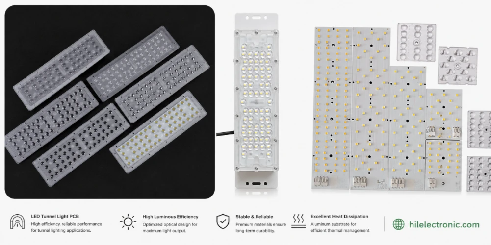
LED Tunnel Light PCB Manufacturing — High-Reliability Engines & Drivers
Figure 1. LED tunnel light PCB production and assembly...
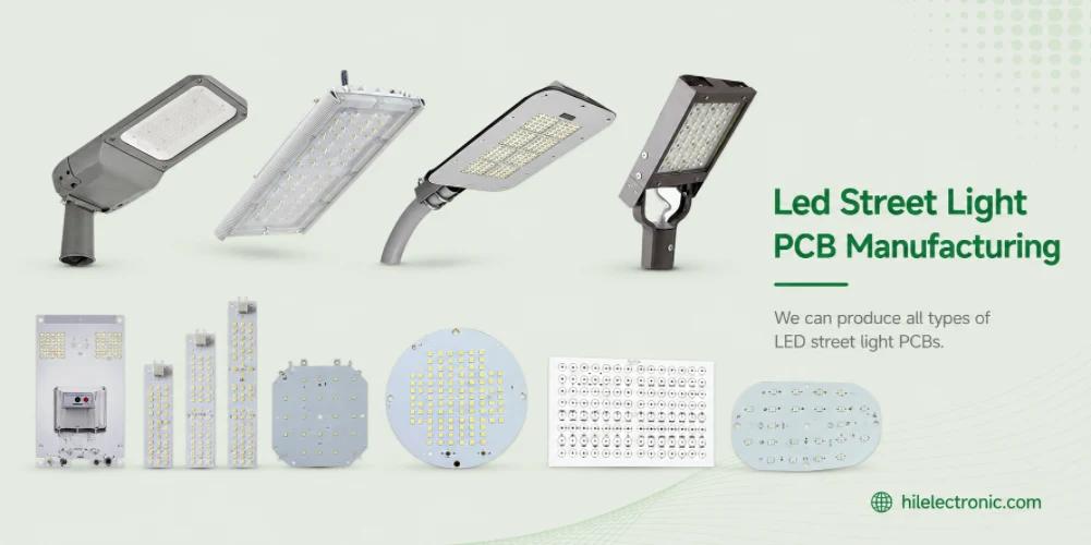
LED Street Light PCB Manufacturing & Assembly by Highleap Electronics
Figure 1. LED street light PCB production and assembly...
LED Wall Washer PCB Manufacturing — RGBW Light Engines & DMX Pixel Control
Figure 1. LED wall washer PCB production and assembly...

8 Steps to Manufacture a Perfect Aluminum PCB
Figure 1. Aluminum Pcb manufacturing reference for PCB...
How to get a quote for PCBs
Let us run DFM/DFA analysis for you and get back to you with a report.
You can upload your files securely through our website.
We require the following information in order to give you a quote:
-
- Gerber, ODB++, or .pcb, spec.
- BOM list if you require assembly
- Quantity
- Turn time