
Back to blog
8-layer PCB Standard Stacking Technology and Design Challenges

The world of electronics heavily relies on Printed Circuit Boards (PCBs) for various applications. Among the diverse range of PCBs available, the 8-layer PCB stands out as one of the most popular and versatile options. While these boards come with their unique set of advantages and challenges, they remain a preferred choice in the electronics industry due to their ability to meet the stringent requirements of signal integrity. In this comprehensive article, we will delve deep into the intricacies of 8-layer PCBs, exploring how they function, essential design guidelines, and the intricacies of prototyping.
Understanding the 8-Layer PCB Stackup
An 8-layer PCB, as the name suggests, is a multilayer circuit board consisting of four signal layers and four planes, meticulously stacked to form a complex yet highly functional board. These layers comprise ground planes, power planes, and signal layers, with the ground and power planes acting as separators between the signal layers. This precise arrangement serves a dual purpose: it minimizes crosstalk between signal layers and provides inter-plane capacitance, which significantly enhances signal integrity.
An exemplary 8-layer PCB stackup provides ample routing space, accommodating multiple power islands and enabling the miniaturization of complex devices while improving operational speed. Unlike simpler PCBs, which may have only two conductive layers, 8-layer PCBs incorporate more than four layers of conductive materials, resulting in improved signal traces and overall efficiency.
The connections between layers in an 8-layer PCB stackup are robust and dependable, ensuring reliable circuit functionality. The presence of additional layers in this configuration contributes to enhanced Electromagnetic Compatibility (EMC) performance and facilitates more sophisticated routing.
Anatomy of an 8-Layer Stackup
An 8-layer stackup consists of four plane layers and four signal layers, each playing a pivotal role in the board’s overall functionality. The distribution of these layers adheres to a balanced structure, often involving one or more prepregs and cores.
Prepregs, subjected to high heat during the fabrication process, firmly bond the layers together to create a cohesive board. Cores, typically made of glass-reinforced epoxy laminate, vary in thickness, typically ranging from 0.1mm to 0.3mm.
Typical Arrangements on an 8-Layer Stackup
Various configurations of planes and signal layers can be employed in an 8-layer PCB stackup, depending on the specific requirements of the intended application. The following are some common arrangements:
Type 1
- Signal 1
- Ground
- Signal 2
- Power
- Ground
- Signal 3
- Power
- Signal 4
In this configuration, there are four signal layers, two ground planes, and power planes. The power and ground planes effectively separate the signal layers. This arrangement ensures that all signal layers have access to at least one power plane. The presence of ground and power planes contributes to significant inter-plane capacitance. Notably, if power islands in the system are positioned close to the bottom layer, they may not effectively ground capacitance. Additionally, the power plane serves as the return path for high-speed signals in signal 4.
Type 2
- Signal 1
- Ground
- Signal 2
- Ground
- Power
- Signal
- Ground
- Signal 4
In this stackup, the planes are situated in the center. This configuration facilitates a closely coupled power and ground plane pair, offering excellent signal integrity.
Type 3
- Signal 1
- Ground
- Power
- Signal 2
- Signal 3
- Ground
- Power
- Signal 4
This arrangement is designed to eliminate potential crosstalk between signal 2 and signal 3. Here, the signal layers are adjacent to planes, ensuring close coupling. Signal 2 and Signal 3 are both sandwiched between planes, effectively shielding them and reducing emissions from the signal layers. This stackup includes two ground planes, which helps reduce ground impedance.
Type 4
- Ground
- Signal 1
- Ground
- Signal 2
- Signal 3
- Power
- Signal 4
- Ground
In this configuration, the ground planes serve as both the top and bottom layers. Additionally, three ground planes are present, with two functioning as outer layers. In this setup, all routing layers are positioned between planes, providing a shield for the routing layers.
Functions of Ground and Power Planes in 8-Layer Stackup
The ground and power planes play critical roles in the functionality of an 8-layer PCB stackup and require careful consideration during the design and manufacturing process. Here are some key functions of these planes:
1. Providing a Clear Return Path
In an 8-layer PCB, the ground plane serves as a clear and efficient return path for signals. Without a well-defined return path, signals can generate Electromagnetic Interference (EMI), adversely affecting the performance of the board.
2. Ensuring Stable Reference Voltages
Stability in reference voltages is paramount for the proper operation of electronic components on the circuit board. Nearly all components on the board connect to a power net, and the return voltage travels back through the ground net. Wider traces are typically used for routing ground nets, and the ground plane simplifies the connection of every component to the ground net.
3. Controlling Crosstalk
As signal speeds increase in electronic circuits, digital components switch positions more rapidly. This can lead to noise pulses traveling through the ground circuit, potentially impacting other parts of the circuit. Ground planes effectively minimize noise and interference, contributing to improved signal quality.
4. Enhancing Electrical Performance
Ground planes and power planes enable manufacturers to regulate the electrical performance of a circuit. Placing a ground plane between two signal layers effectively eliminates crosstalk between them, while the presence of both power and ground planes can significantly enhance the signal integrity of the board.
Tips for 8-Layer PCB Design
While it is tempting to believe that an 8-layer PCB can effortlessly solve all Electromagnetic Interference (EMI) problems, the reality is more complex. Designing an effective 8-layer stackup can be a challenging endeavor. Several key design techniques are essential for achieving a functional 8-layer PCB:
1. Impedance Control
Impedance control is a critical aspect of successful 8-layer PCB design. Designers should measure the impedance of certain traces during the PCB design process. Achieving impedance control involves matching the properties of the substrate material with the locations and dimensions of the traces. It is imperative to ensure that the impedance of the signal traces falls within the specified value, as proper impedance control significantly contributes to overall board performance.
2. Signal Shielding
Effective signal shielding is crucial in 8-layer PCB design. Designers must take measures to shield the signal layers from each other to prevent signal loss and interference. This shielding capability is one of the primary reasons 8-layer PCBs are preferred in complex electronic systems. The additional planes in the stackup act as shields for the signal layers, enhancing overall signal integrity.
3. Prevention of Noise Decoupling
Preventing noise decoupling is a key consideration during the design of an 8-layer stackup. It is essential to take proactive measures to prevent noise decoupling issues. One effective strategy is the creation of a digital ground plane, which facilitates the design of multiple ground and power planes that can be distributed throughout the stackup, reducing the risk of noise decoupling.
4. Layer Balancing
Layer balancing is a critical aspect of designing a robust PCB stackup. A balanced 8-layer stackup ensures that the cross-sectional structure and layer surfaces of the circuit are symmetrical. Designers should identify and address areas that may deform due to manufacturing stresses, emphasizing the need for a thorough review of the circuit layout. A symmetrical stackup enhances the board’s reliability and performance.
Important Considerations for 8-Layer Stackup Fabrication
The fabrication process of an 8-layer PCB stackup involves several critical considerations to ensure the final product meets the required standards:
1. Stackup Measling
Stackup measling is a common issue encountered during the fabrication of 8-layer PCBs. To mitigate this problem, manufacturers can use silicon pads and epoxy plates during the board arrangement process. This helps maintain uniform thickness throughout the board, eliminating the risk of measling.
2. Interlayer Offset
During fabrication, there is a possibility of interlayer offset, which can lead to misalignment of internal layers in an 8-layer PCB. Manufacturers can address this issue by implementing rivet dowel methods in board designs, ensuring precise layer alignment and reducing the likelihood of offset.
3. Core Materials Selection
Choosing the right core material is crucial for the fabrication of an 8-layer PCB stackup. Some core materials can pose challenges during fabrication, so careful selection is necessary to avoid complications and ensure a successful manufacturing process.
4. Bow and Twist Control
Bow and twist control are vital for maintaining the flatness of multilayer boards. Bow and twist issues can arise from uneven copper distribution, potentially causing electrical components and parts to shift during assembly. Designing and fabricating layer stackups with symmetry helps mitigate bow and twist problems, ensuring the board’s dimensional stability.
How to Choose the Best 8-Layer PCB Manufacturer
The functionality and quality of your 8-layer PCB stackup greatly depend on the manufacturer you choose. Selecting the right manufacturer is a crucial decision, and several factors should be considered:
1. Expertise
Evaluate the manufacturer’s expertise, including their experience and skill in producing 8-layer PCBs. Given the complexity of these stackups, partnering with a skilled and experienced manufacturer is essential. Inquire about the manufacturer’s track record, certifications, and the relevance of their experience to your specific requirements.
2. Turnaround Time
Consider the manufacturer’s turnaround time, which refers to the duration required to complete the design and fabrication of your circuit boards. Ensure that the selected 8-layer PCB manufacturer can meet your project’s timeline efficiently and effectively. Reviewing feedback from past clients can provide insights into the manufacturer’s adherence to promised turnaround times.
3. Order Capacity
Assess whether the 8-layer PCB manufacturer can accommodate the quantity of boards you require. Some manufacturers may have limitations in terms of production volume. If your project involves the production of a large quantity of 8-layer stackups, ensure that the manufacturer can meet your specific order capacity needs.
4. Customer Service
Effective communication and responsiveness are vital aspects of excellent customer service. A reliable 8-layer stackup manufacturer should be readily available to address your inquiries and provide guidance throughout the production process. Evaluate the manufacturer’s customer service reputation and responsiveness to ensure a smooth collaboration.
Why Use an 8-Layer PCB Stackup
8-layer PCB stackups offer a multitude of benefits that make them the preferred choice for various applications in the electronics industry. The unique advantages of 8-layer stackups include:
1. Improved Signal Integrity
One of the primary advantages of using an 8-layer PCB stackup is the substantial improvement in signal integrity. These stackups are designed to maximize the functionality of electronic devices by minimizing signal interference and distortion. The inclusion of multiple ground and power planes acts as a shield for the four signal layers, effectively reducing Electromagnetic Interference (EMI) and enhancing signal quality.
2. EMI Reduction
Complex electronic devices often generate Electromagnetic Interference (EMI) that can disrupt neighboring circuits. 8-layer stackups are well-suited for such applications as they can significantly reduce or eliminate EMI through careful arrangement and shielding of signal layers. This reduction in EMI ensures the reliable operation of sensitive electronics.
3. Cost-Efficiency
8-layer PCB stackups offer cost-efficiency, both in terms of manufacturing and long-term operation. These stackups are known for their durability and low maintenance requirements, resulting in cost savings over the lifetime of electronic devices. Additionally, their compact design helps save valuable board space.
Conclusion
The design and manufacturing of an 8-layer PCB stackup require a systematic and meticulous approach. 8-layer stackups are widely employed in the electronics industry, especially in complex devices, due to their exceptional Electromagnetic Compatibility (EMC) performance and signal routing capabilities. When collaborating with an 8-layer PCB manufacturer, it is imperative to prioritize functionality and quality to meet the demanding requirements of modern electronic applications. A well-designed and properly fabricated 8-layer stackup can be the foundation for reliable and high-performance electronic systems.
For production planning, it also helps to compare this topic with PCB quality assurance process and circuit protection in PCB design before finalizing the fabrication or assembly package.
PCB & PCBA Quick Quote
Related Articles
EAGLE CAD in 2026: End of Life, Free-Version Limits, and Where to Go Next
EAGLE CAD shaped a generation of PCB designers, but in 2026 the single most important fact about it is that it is ending. Autodesk retires EAGLE on June 7,.
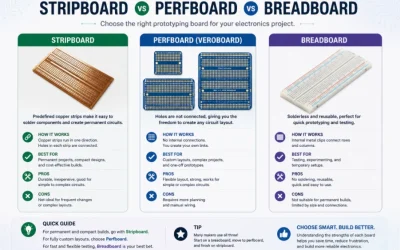
Stripboard vs Perfboard vs Breadboard: Which Prototyping Board to Use and When
Breadboard, stripboard, and perfboard solve three different stages of building a circuit — testing an idea, making a permanent simple build, and making a.
EAGLE vs KiCad in 2026: Why the Comparison Now Has a Clear Winner
For years, EAGLE vs KiCad was a genuine debate — EAGLE’s polish and community libraries against KiCad’s freedom and price. In 2026 that debate is.