
Circuit Board Reverse Engineering Services

Table of Contents
- Why Boards End Up Without Documentation
- What the Service Actually Produces
- The Hard Variables: What Slows a Project Down
- Firmware, ASICs, and What Cannot Be Recovered
- Cost and Timeline: What the Numbers Depend On
- How to Avoid Getting Locked In by the Wrong Provider
- Highleap’s Circuit Board Reverse Engineering Services
- Frequently Asked Questions
The board that keeps the production line running has failed. The original manufacturer closed in 2011. The design files were never transferred. The only path forward — short of replacing the entire system at six-figure cost — is to reproduce the board from the physical unit still in hand.
That is the situation most organizations are in when they look for circuit board reverse engineering services. Not academic curiosity. A specific problem, with real downtime and real cost attached to it.
This guide covers what a professional PCB reverse engineering engagement actually delivers, what makes projects harder than they look, what cannot be recovered, what it costs, and how to choose a provider who won’t leave you worse off than when you started.
1. Why Boards End Up Without Documentation
Understanding why documentation disappears helps set realistic expectations for what reverse engineering can and cannot reconstruct.
The most common reasons design files no longer exist:
- Original manufacturer closure: The contract manufacturer or design house that built the board closed, was acquired, or discontinued the product line. Files were not transferred — or were transferred incompletely.
- Data loss during corporate transitions: Acquisitions, mergers, and facility moves are the most frequent cause of lost design data in industrial and medical equipment sectors. A board designed in 1995 may have changed hands three times before anyone realized the files were gone.
- Deliberate withholding: Some original manufacturers retain design files as a commercial lever — the only way to get replacement boards is to buy them from the OEM. Circuit board reverse engineering breaks that dependency.
- Never documented in the first place: Prototype-to-production transitions at small companies often skip formal documentation. The engineer who designed the board is gone, and what remains is a working unit and nothing else.
- Format obsolescence: Files exist but are in software versions or formats no longer readable by any current tool — functionally lost even though physically present.
In all of these cases, the physical board is the primary source of truth. Everything the reverse engineering process produces is reconstructed from that physical evidence.
2. What the Service Actually Produces
A circuit board reverse engineering engagement produces a complete documentation package — the same set of files that would exist if the board had been designed from scratch in-house. The key outputs:
| Deliverable | Format | What It Enables |
|---|---|---|
| Schematic diagram | PDF + native CAD (Altium, KiCad, OrCAD) | Circuit understanding, fault diagnosis, future modifications |
| Gerber files (all layers) | RS-274X / Gerber X2 | Board fabrication at any manufacturer |
| Drill files | Excellon format | Hole drilling during fabrication |
| Bill of Materials | Excel / CSV | Component procurement; obsolescence substitution |
| Netlist | IPC-D-356 or native CAD | Electrical testing, design verification |
| Pick-and-place file | CSV with X/Y coordinates and rotation | Automated SMT assembly |
| Assembly drawing | Manual assembly reference and incoming inspection |
How the schematic gets reconstructed is the part most clients don’t see but care about most. Engineers don’t just trace copper — they analyze the circuit topology: identify the power supply architecture, map the processor I/O, trace the analog signal chain, and document what each section is doing functionally. A schematic extraction that only shows connections without functional understanding produces a document that’s technically complete but practically useless for troubleshooting or modification.
What prototype validation means for you: The documentation package is only confirmed correct when a board fabricated from the Gerber files and assembled from the BOM powers up and functions identically to the original. Any discrepancy — a missed trace, a wrong component value, an incorrect via assignment — shows up here, before you receive the files. Without prototype validation, you are receiving an unverified reconstruction.
Optional deliverables available from full-service providers:
- Firmware binary (where technically and legally extractable — see Section 4)
- Obsolete component substitution recommendations with modern equivalents
- STEP 3D model for mechanical integration verification
- Fabricated and tested replacement boards as part of the engagement
3. The Hard Variables: What Slows a Project Down
Every circuit board reverse engineering project looks straightforward until it isn’t. These are the variables that extend timelines and increase cost — worth knowing before you submit a board for analysis.
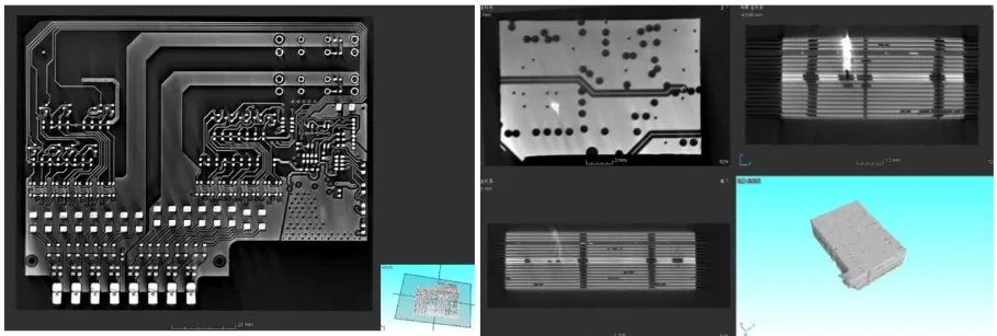
Layer count is the primary cost and time driver. Outer layers are imaged optically. Inner layers on a 4+ layer board require X-ray imaging or CT scanning. An 8-layer board is not 4× the work of a 2-layer board — it is 6–8× due to inter-layer connectivity that must be traced and verified across every layer combination. For HDI boards with microvias and blind/buried vias, CT scanning is required because X-ray cannot resolve stacked via structures.
Unmarked or custom components are the most unpredictable variable. A sanded-off IC marking or a custom ASIC with no public documentation can require days of functional analysis — curve tracing, behavioral testing, and sometimes decapsulation — to identify what the component is and what it does. A single unidentifiable custom IC can add 1–2 weeks to a project.
Board damage forces inference instead of observation. A burnt trace, a corroded section, or missing components require engineers to reconstruct what was there from the surrounding circuit context. This is engineering judgment, not measurement — it adds uncertainty and requires functional validation to confirm the inference was correct.
Board condition factors that increase project scope:
- Conformal coating or encapsulant covering component markings or traces
- Rework wires or cut traces indicating field modifications (which version is correct?)
- Previous repair attempts that have altered the original circuit
- Corrosion from moisture or chemical exposure obscuring pad connections
- Only one sample board available — if destructive layer analysis is needed, you lose the only reference unit
Providing at least two sample boards — one for non-destructive analysis and one that can be used for destructive cross-section if required — significantly reduces project risk and timeline.
4. Firmware, ASICs, and What Cannot Be Recovered
This is the section most circuit board reverse engineering service pages skip. It matters more than any other part of the evaluation.
Microcontroller firmware is not part of the PCB — it is software programmed into the device. The reverse engineering process reconstructs the hardware design perfectly and says nothing about what program is running on the MCU. If the MCU is blank or erased, a reproduced board will power up and do nothing. Firmware extraction is a separate process that requires reading the programmed code from the device.
Whether firmware can be extracted depends entirely on the MCU’s read protection:
- No read protection set: Firmware can be read directly with a programmer. Common on older designs from the 1990s–2000s.
- Software read protection (RDP): Most modern MCUs (STM32, PIC, AVR, etc.) allow the developer to set a read-protection bit. Once set, the firmware cannot be extracted by any standard means without destroying the device.
- Hardware security: Secure elements and crypto-enabled MCUs have physical countermeasures that make extraction extremely difficult or impossible without specialized lab equipment that costs tens of thousands of dollars per attempt.
If your board’s MCU has read protection enabled — which most production boards do — a reverse engineering service cannot extract the firmware. The board documentation will be complete and accurate, but the MCU will need to be reprogrammed with firmware you either retain or reconstruct from scratch.
Custom ASICs and FPGAs present a similar problem. The physical package can be identified, the pinout can be characterized by functional testing, and the interface to the ASIC can be documented. But the internal logic — what the ASIC actually does — is a black box. A reproduced board containing the same ASIC will function correctly as long as the original ASIC is available. If the ASIC is no longer manufactured and cannot be sourced, the board cannot be reproduced in functional form regardless of how complete the reverse engineering documentation is.
The honest answer before you engage any circuit board reverse engineering service: Identify every programmable device on the board, determine whether firmware extraction is needed, and ask the provider specifically what their capability and success rate is for your MCU family. A provider that guarantees firmware extraction for read-protected MCUs without caveats is not being honest with you.

5. Cost and Timeline: What the Numbers Depend On
| Complexity Level | Typical Profile | Cost Range | Timeline |
|---|---|---|---|
| Low | 1–2 layers, 20–100 components, all identifiable, no HDI | $3,000–$5,000 | 2–3 weeks |
| Medium | 4–6 layers, 100–500 components, 1–5 custom parts | $5,000–$15,000 | 3–6 weeks |
| High | 8–16+ layers, 500–2,000+ components, HDI, custom ASICs | $15,000–$50,000+ | 6–12 weeks |
What pushes a project from medium to high cost — and why:
Each additional board layer is not an incremental addition. It requires a separate imaging pass, a complete trace routing exercise for that layer, and verification against all other layers. An 8-layer board has 28 possible layer-pair combinations to check for connectivity — compared to 1 for a 2-layer board.
Prototype fabrication and functional validation, if included in the engagement, adds $500–$3,000 depending on board complexity — but it is the only way to confirm the reconstruction is correct before you take ownership of the files.
How to get an accurate quote on the first request:
Submit photographs of both sides of the board at sufficient resolution to read component markings, the board’s approximate dimensions and visible layer count from the edge, any known information about the board’s function or original manufacturer, the specific deliverables you need (documentation only, or documentation plus prototype boards), whether firmware extraction is needed, and how many sample boards you can provide. Incomplete submissions produce range quotes that are too wide to act on.
6. How to Avoid Getting Locked In by the Wrong Provider
This section exists because there is a specific practice in the circuit board reverse engineering industry that costs clients significantly more than the initial quote suggested — and it is worth knowing about before you hand over your board.
File locking: Some providers deliver Gerber files that appear complete but contain deliberate errors — traces routed to wrong nets, missing vias, incorrect pad sizes — that make the board unfabricable at any other manufacturer while appearing fine in a viewer. The only way the client can get working boards is to go back to the provider for fabrication. The reverse engineering service was priced low; the fabrication markup is where the margin comes from.
How to protect yourself:
- Require that your deliverable files work correctly at any manufacturer — put this in the contract before the project starts
- Run a DRC check on received Gerber files before accepting delivery
- Prototype validation at a manufacturer other than the reverse engineering provider confirms the files are genuinely correct
- Request files in standard open formats (RS-274X Gerber, Excellon drill, native CAD) — proprietary formats create dependency
Provider evaluation checklist:
- ☐ NDA executed before you send the board — your hardware design is your intellectual property and should be protected from the first contact
- ☐ In-house imaging capability: high-resolution optical scanning, X-ray, and CT scanning for multilayer and HDI boards
- ☐ Prototype validation included or available as an add-on — reconstruction verified by a functional board, not just visual comparison
- ☐ In-house PCB fabrication and assembly for validation — means the provider can verify the files are correct before delivering them
- ☐ Transparent pricing with all costs stated upfront — no “complexity surcharges” added after the project begins
- ☐ Component sourcing capability for obsolete parts — especially relevant if the original BOM includes end-of-life devices
- ☐ ISO 9001 certification as a minimum quality baseline
Red flags that should stop the evaluation immediately:
- Quote dramatically lower than two or more other providers for the same scope — the shortfall will appear somewhere
- No prototype validation offered, described as “unnecessary for simple boards” — it is always necessary for confidence in the reconstruction
- Reluctance to commit to standard file formats in the contract
- No NDA process — a provider unwilling to sign a confidentiality agreement before receiving your proprietary board is not protecting your interests
7. Highleap’s Circuit Board Reverse Engineering Services
Highleap Electronics provides end-to-end circuit board reverse engineering services with integrated manufacturing — board analysis through functional validation under one roof.
What makes integrated capability matter: When the provider doing the reverse engineering also fabricates and assembles the prototype, they are motivated to get the files right — their own manufacturing process validates the work. Providers who only do documentation and outsource fabrication have a weaker feedback loop on file accuracy.
Capability overview:
- Board analysis: High-resolution optical scanning, X-ray inspection, and CT scanning for boards up to 16+ layers including HDI with blind/buried via structures
- Schematic extraction: Full circuit reconstruction with functional block identification — not just connectivity mapping
- BOM reconstruction: Component identification including custom and unmarked parts; obsolete component sourcing with modern substitution recommendations
- Layout reconstruction: Gerber files, drill files, pick-and-place data in standard open formats — verified correct at any manufacturer
- Prototype validation: Boards fabricated and assembled in-house; functional testing against original board behavior before file delivery
- Protection: NDA executed before board receipt; ISO 9001:2015 certified
- Timeline: 3–8 weeks depending on complexity; rush service available for critical equipment downtime situations
Request a Reverse Engineering Quote
Frequently Asked Questions
What information do I need to provide to get a circuit board reverse engineering quote?
Photographs of both sides of the board at enough resolution to read component markings, approximate board dimensions and layer count from the edge, any known information about the original manufacturer or function, the deliverables you need (documentation only or documentation plus prototype boards), whether firmware extraction is required, and how many sample boards are available. Complete submissions produce accurate quotes; incomplete submissions produce ranges too wide to compare or act on.
Can a circuit board reverse engineering service extract firmware from a microcontroller?
Only if the MCU does not have read protection enabled. Older devices from the 1990s–2000s often have no read protection and firmware can be read directly with a programmer. Most modern production MCUs — STM32, PIC, AVR, and similar families — have read-protection bits set during manufacturing. Once set, firmware extraction is not possible by standard means. A provider that guarantees firmware extraction for read-protected devices without qualification is not being accurate. Identify the MCU family and read protection status before assuming firmware can be recovered.
What happens if a component on the board can no longer be purchased?
The reverse engineering process documents the component’s specifications — electrical parameters, package type, pinout, and function. With that information, modern equivalent components can be identified. In most cases, a functionally equivalent replacement exists from current production. The exception is custom ASICs designed specifically for the original product — if the ASIC is unavailable and cannot be second-sourced, the board cannot be reproduced without a redesign that replaces the ASIC function with programmable logic or an equivalent circuit. This is a separate engineering engagement, not part of standard circuit board reverse engineering.
How do I know the reverse engineered files are actually correct?
The only reliable confirmation is prototype validation — fabricating a board from the reconstructed Gerber files, assembling it with the reconstructed BOM, and verifying that it functions identically to the original. Visual comparison of board photographs to the reconstructed layout catches gross errors but misses subtle connectivity issues that only appear when the board is powered. Require prototype validation as a condition of delivery, not an optional add-on.
Is reverse engineering a competitor’s circuit board legal?
Reverse engineering of electronic products for the purpose of interoperability, replacement, or competitive analysis is generally legal in most jurisdictions, including the United States and European Union, under established principles of fair use and right to repair. However, reproducing a competitor’s product for sale — particularly if it copies trade dress or violates patent claims — is a different matter. The legality of any specific project depends on jurisdiction, purpose, and the intellectual property status of the original design. Consult legal counsel before proceeding with competitive analysis projects.
How many sample boards should I send for analysis?
Send at least two if you can. One board can be reserved for non-destructive analysis; the second can be used for destructive cross-section if inner layer imaging requires it. If only one board is available, inform the provider upfront — this constrains the analysis options and may affect timeline and cost. For boards where no functional unit survives (only a damaged or incomplete specimen), provide that information in the initial quote request so the scope reflects the reconstruction difficulty.

Recommended Posts
LED High Bay Light PCBs: Metal-Core Light Engines, Drivers & Turnkey Boards Built to Spec
Figure 1. LED high bay light PCB manufacturing reference....
LED Linear & Strip Light PCBs: Long-Format Engines, Flexible & Rigid-Flex Boards
Figure 1. LED linear light PCB manufacturing reference....

LED Grow Light PCBs: Multi-Channel Spectrum Boards, Drivers & Thermal Design
Figure 1. LED grow light PCB manufacturing reference....
Explosion-Proof LED Light PCBs: Hazardous-Location Boards, Drivers & Assembly
Figure 1. explosion-proof LED light PCB manufacturing...
How to get a quote for PCBs
Let us run DFM/DFA analysis for you and get back to you with a report.
You can upload your files securely through our website.
We require the following information in order to give you a quote:
-
- Gerber, ODB++, or .pcb, spec.
- BOM list if you require assembly
- Quantity
- Turn time