
Back to blog
PCB Reverse Engineering Service for Obsolete and Custom PCBs

In this article, we explain the PCB reverse engineering process step by step, covering practical methods, tools, and real-world applications to help achieve accurate and functional duplication.
PCB Reverse Engineering Process Explained
Obtain the Target PCB
The first and foremost step in circuit board reverse engineering is to obtain the target PCB. This could be a PCB from a competitor’s product, a legacy device, or any PCB where the original design documentation is not available. It’s essential to obtain the physical PCB, as it serves as the starting point for the reverse engineering process.
During this step, it’s crucial to document the layout of the PCB thoroughly. This documentation involves photographing the entire board and diagramming all component positions, orientations, and details on paper. Special attention should be given to critical components such as diodes, transistors, integrated circuits (ICs), and any other components that play a significant role in the board’s functionality.
Component Removal and Scanning
Once the PCB layout is documented, the next step is to remove all the components from the PCB. This process requires desoldering each component carefully to ensure that they can be reattached later if needed. Proper handling and labeling of components are essential to avoid confusion during the reassembly phase.
After the components are removed, the PCB needs to be thoroughly cleaned. Isopropyl alcohol is often used to clean the board and remove any residual solder, flux, or contaminants.
With the board cleaned and components safely stored, the PCB is ready for scanning. High-resolution scanning is critical in this step, with a scanner set at 600 DPI (dots per inch) or higher being commonly used. Before scanning, it’s recommended to gently polish the copper layers on the PCB to make them shine. The PCB’s top and bottom layers should be scanned separately in high-resolution color, ensuring that the board lies flat on the scanning surface for accurate results.
Image Processing and Optimization
Once the PCB scans are obtained, they are imported into image processing software such as Adobe Photoshop. In this software, various adjustments are made to enhance the visibility of the copper traces and make them distinct from the substrate. This typically involves adjusting the levels, contrast, and brightness to improve image clarity.
The bottom layer scan is often converted to black-and-white for better visibility of the traces. Close examination is required to ensure that the scan captures all tracings sharply and without any disconnections.
The optimized layers are then saved as BMP (bitmap) files, typically named “TOP” and “BOTTOM” to denote the top and bottom PCB layers, respectively. Specialized software may also be employed to correct any trace defects or anomalies evident in the scans.
PCB Design Software Integration
The BMP files containing the optimized PCB scans are opened in PCB design software. These files need to be converted into the native format of the design software to proceed with the reverse engineering process.
Alignment tools within the software are utilized to overlay pad holes, vias, and matching points between layers with precision. Any significant deviations or misalignments should be addressed promptly, as accuracy is paramount in this phase.
Tracing and Replication
The tracing and replication phase is where the reverse engineering truly begins. Engineers start by working with the top layer scan, tracing out all visible design elements to recreate the layer digitally. Component placements are matched with the earlier documentation photographs, and connections are routed following the scans to replicate the copper traces electrically.
Once the vector tracing is complete for the top layer, the original scan layer is deleted to leave only the digitally recreated elements. This process is then repeated for the bottom scan layer, using connectivity tools to validate connections between layers. Additionally, filled zones are added to represent any internal ground or power planes present on the PCB. For complex multi-layer boards, transparency display modes and alignment guides are often used to match vias between layers accurately.
Validation and Testing
After the digital recreation of the PCB is completed, the next crucial step is validation and testing. This involves printing 1:1 scale top silkscreen and bottom layer films from the digital files. These printed films are then carefully overlaid onto the target PCB, which is backlighted to facilitate a visual comparison. The goal is to ensure a perfect alignment of all elements on the printed films with the actual board.
Any errors or discrepancies detected during this validation phase should prompt further modifications to the digital traces until full validation is achieved. This phase helps ensure the accuracy of the reverse-engineered PCB.
Functional Duplication
The final step in PCB reverse engineering is functional duplication. With the form and function accurately captured and validated to match the original PCB, the reverse-engineering process is considered complete.
In this phase, boards are populated with components based on the digitally recreated data. These newly constructed boards are then subjected to functional testing and benchmarking. The goal is to verify electrical parity and validate the true functional duplication of the original PCB.
PCB reverse engineering is a complex and challenging process that involves meticulous documentation, precise scanning, image processing, digital recreation, and thorough validation. When executed correctly, it offers numerous benefits, from remanufacturing obsolete PCBs to enabling custom modifications and fostering technological progress.
It’s important to note that while PCB reverse engineering can be a powerful tool, it should always be conducted ethically and within the bounds of intellectual property rights and legal regulations. Responsible reverse engineering can contribute to innovation and advancement in the electronics industry while respecting the rights of original designers and manufacturers.

Benefits of Printed Circuit Board Reverse Engineering
Printed circuit board (PCB) reverse engineering offers practical and strategic advantages for manufacturers and product developers. It is widely used to support legacy hardware, reduce development costs, and enable continued innovation when original design data is unavailable.
-
Remanufacturing of Obsolete PCBs:
PCB reverse engineering makes it possible to recreate discontinued or obsolete circuit boards when the original equipment manufacturer (OEM) no longer provides support or replacement parts. This allows companies to restore functionality and extend the service life of critical equipment, especially in industries such as industrial automation, defense, and transportation. Once the design is recovered, the board can be prepared for reliable PCB production using modern manufacturing processes. -
Simplified PCB Repair and Failure Analysis:
As electronic systems age, component wear, environmental stress, and electrical degradation can lead to failures. Reverse engineering helps engineers understand the original circuit structure, making fault diagnosis more efficient. With accurate design data restored, damaged boards can be repaired or rebuilt and then assembled through professional circuit board assembly services, reducing downtime and maintenance costs. -
Custom Modifications and Design Improvements:
By reconstructing schematics and PCB layouts, reverse engineering enables targeted design modifications. Engineers can optimize performance, add new features, or adapt the board for updated components and new applications. This is especially valuable in sectors such as medical devices and automotive electronics, where customization and long-term product evolution are essential. -
Cost Reduction for Low-Volume Production:
For small-batch or niche products, developing a PCB from scratch can be expensive and time-consuming. Reverse engineering significantly lowers upfront engineering costs by leveraging an existing design. After validation, the recovered design can be efficiently manufactured and assembled as part of a streamlined electronics manufacturing solution, making low-volume production economically viable. -
Improved Interoperability and Compatibility:
Reverse engineering provides insight into how existing products function and interact with other systems. This understanding helps engineers design compatible interfaces, improve interoperability, and ensure seamless integration with related hardware or infrastructure, which is critical in communication and industrial control systems. -
Support for Responsible Technological Progress:
When conducted ethically and within legal boundaries, PCB reverse engineering contributes to technological advancement. It enables the study of proven designs, supports knowledge transfer, and helps organizations maintain and improve complex electronic systems while respecting intellectual property rights.

Unlock New Possibilities with PCB Reverse Engineering for Custom Solutions
At Highleap Electronics, we take PCB reverse engineering beyond replication. While it’s an excellent tool for recreating obsolete PCBs, it also opens doors to customized solutions that meet your specific needs. Whether you’re developing new features for existing products, improving performance, or optimizing designs for unique applications, reverse engineering allows you to make precise changes and modifications to the design. Our experienced team ensures that your modifications are tailored to your exact specifications, giving you a competitive edge in your market. With Highleap, you can unlock new potential for your electronics, driving innovation and enhancing the capabilities of your products.
Cost-Effective Solutions for Small-Scale and Niche Production Runs
PCB reverse engineering is a powerful tool for businesses needing to replicate PCBs for small-scale production runs. At Highleap Electronics, we understand that high initial costs can be a barrier for startups and niche product developers. Our reverse engineering services significantly reduce costs by allowing you to reproduce PCBs without the need for expensive new designs. Whether you’re looking to produce low-volume custom parts or replace outdated electronics, we offer cost-effective solutions that meet your specific requirements. With our precise reverse engineering techniques, you can manufacture small runs of high-quality, reliable PCBs tailored to your product’s unique specifications, all while reducing costs and lead times.
Highleap Provides Reliable PCB Reverse Engineering Service
With nearly two decades of experience in the PCB industry, Highleap Electronics delivers reliable and professional PCB reverse engineering services for customers facing obsolete hardware, missing design files, or urgent replacement needs. In addition to PCB design and assembly capabilities, our engineering team focuses on restoring functional, manufacturable, and compliant PCB designs from existing circuit boards.
For projects that require rapid turnaround, PCB reverse engineering is often combined with fast PCB duplication solutions to help customers minimize downtime and accelerate product recovery. This approach is especially effective for legacy systems, discontinued products, and low-volume production scenarios where speed and accuracy are critical.
At the same time, we recognize that intellectual property protection is a key concern in reverse engineering projects. Highleap Electronics follows strict ethical standards and emphasizes responsible practices, ensuring that all activities respect legal boundaries and contractual obligations. Customers who need additional safeguards can also explore our guidance on protecting PCB design assets to reduce the risk of unauthorized copying and IP exposure.
Our goal is to help customers repair, replicate, or enhance outdated electronics while maintaining compliance, reliability, and long-term manufacturability. Contact our team to discuss your custom PCB reverse engineering requirements and leverage our experience to move your project forward with confidence.
This article was updated in January 2026 to reflect current PCB reverse engineering practices.
PCB Reverse Engineering FAQs
Is PCB reverse engineering legal?
PCB reverse engineering can be legal when conducted for legitimate purposes such as repairing obsolete equipment, maintaining legacy systems, ensuring compatibility, or creating replacement boards when original design files are unavailable. However, legality depends on intellectual property rights, contractual agreements, and local regulations. Each project should be evaluated carefully to ensure compliance with applicable laws and ethical standards.
What types of PCBs can be reverse engineered?
PCB reverse engineering can be applied to a wide range of circuit boards, including single-layer, double-layer, and multilayer PCBs. It is commonly used for analog, digital, and mixed-signal designs, as well as legacy or discontinued products where original documentation no longer exists.
How much does PCB reverse engineering cost?
The cost of PCB reverse engineering varies depending on factors such as board complexity, number of layers, component density, and verification requirements. Simple boards typically require less engineering effort, while complex multilayer or high-density designs involve more detailed analysis and validation.
Can you reverse engineer obsolete or discontinued PCBs?
Yes. One of the most common applications of PCB reverse engineering is the replacement of obsolete or discontinued circuit boards. By reconstructing schematics and PCB layouts from existing hardware, functional replacements can be produced even when original manufacturers no longer provide support.
Do you provide PCB fabrication or assembly after reverse engineering?
Yes. After the PCB reverse engineering process is completed, the recovered design data can be used for PCB fabrication and assembly. This allows customers to move directly from reverse engineering to manufacturing, which is especially useful for low-volume production, repairs, or legacy system maintenance.
How long does PCB reverse engineering take?
Project timelines depend on PCB complexity and validation requirements. Simple boards may be completed within several days, while more complex multilayer designs typically require one to several weeks to ensure accurate reconstruction and functional verification.

Recommended Posts

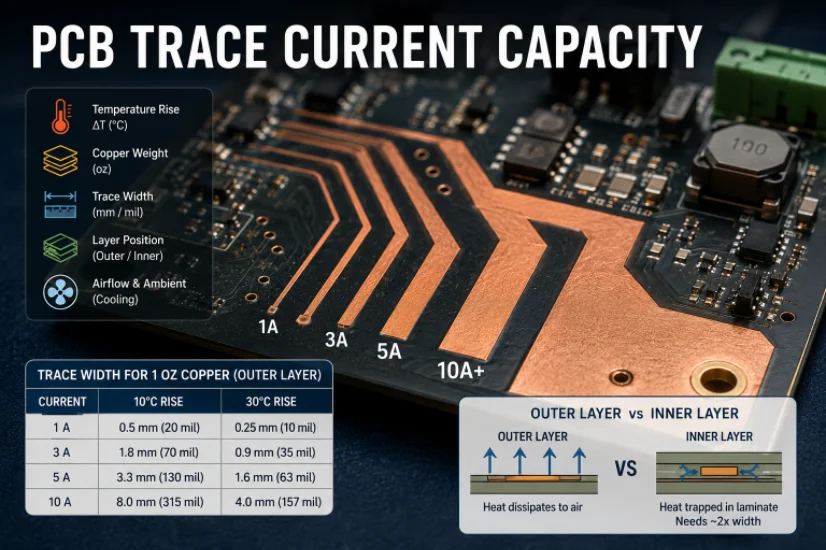
PCB Current Calculator: Sizing Trace Width and Vias with the IPC-2221 Formula
Figure 1. Pcb Current Calculator reference image for PCB...
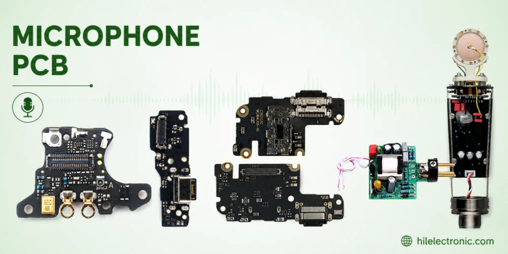
Microphone PCB Design: How the Board Itself Shapes Your Audio Quality
Figure 1. Microphone Pcb reference image for PCB...
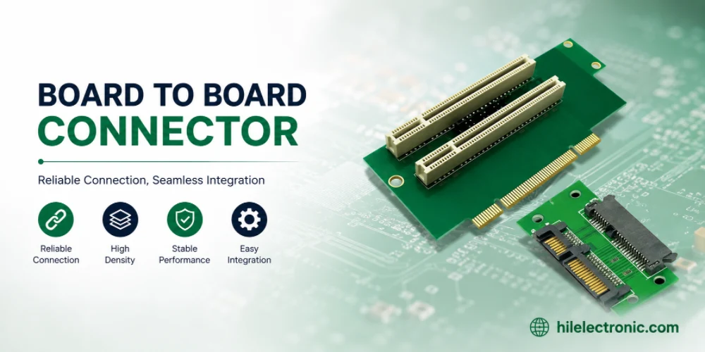
Board-to-Board Connector: Types, Specifications, and How to Select One
Figure 1. Board To Board Connector reference image for PCB...
PCB Trace Width Calculator: How to Size Traces for Current, Voltage Drop, and Impedance
Figure 1. A PCB trace width calculator is a starting point...
How to get a quote for PCBs
Let us run DFM/DFA analysis for you and get back to you with a report.
You can upload your files securely through our website.
We require the following information in order to give you a quote:
-
- Gerber, ODB++, or .pcb, spec.
- BOM list if you require assembly
- Quantity
- Turn time
In addition to PCB manufacturing, we offer a comprehensive range of electronic services, including PCB design, PCBA (Printed Circuit Board Assembly), and turnkey solutions. Whether you need help with prototyping, design verification, component sourcing, or mass production, we provide end-to-end support to ensure your project’s success. For PCBA services, please provide your BOM (Bill of Materials) and any specific assembly instructions. We also offer DFM/DFA analysis to optimize your designs for manufacturability and assembly, ensuring a smooth production process.