
Optical Transceiver PCB Assembly Services in China
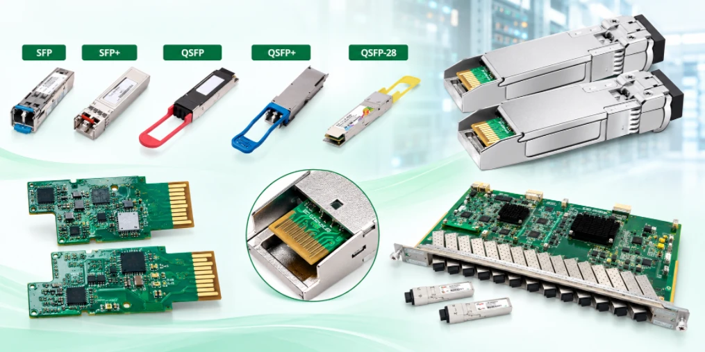
Highleap Electronics provides optical transceiver PCB assembly for OEMs and optical-module electronics manufacturers sourcing populated boards for customer-designed high-speed transceiver products. Our PCBA services can combine bare PCB procurement or fabrication, component sourcing, solder-paste printing, SMT placement, reflow, through-hole operations where specified, assembly inspection and agreed board-level electrical or functional testing.
Optical transceiver PCBAs can be small yet demanding: closely packed ICs, precision passives, module-management circuits, dense power components and mechanically restricted connector areas may leave little allowance for assembly variation. Highleap reviews the BOM, PCB panel requirements, pad and via treatment, component packages, stencil requirements and inspection access before confirming the assembly process. We coordinate the released design with sourcing and production so the assembled boards match the accepted build specification.
We offer turnkey and customer-consigned assembly scopes, with responsibility for components and testing specified in the quotation. Complete optical-engine alignment, transceiver calibration, BER testing and optical-power qualification are separate activities that must be agreed expressly; a standard PCBA quotation should not be mistaken for full optical-module manufacturing.
Table of contents
- Optical Transceiver PCB Assembly Scope and Delivered Product
- Turnkey Component Sourcing, BOM Verification and Material Readiness
- SMT, Fine-Pitch Packages and Assembly Process Engineering
- AOI, X-Ray, Board-Level Testing and Defined Acceptance
- NPI Builds, Engineering Changes and Repeat PCBA Production
- Request an Optical Transceiver PCB Assembly Quote from Highleap
OPTICAL TRANSCEIVER PCBA
Ready to Quote Your Transceiver PCBA?
Submit the BOM, released PCB data, centroid files, test scope and planned build quantities for review.
Request an Optical Transceiver PCBA Quote →Optical Transceiver PCB Assembly Scope and Delivered Product
Highleap assembles customer-designed optical transceiver boards for prototype, pilot and production programs. The project may require fabrication plus assembly from one partner, assembly using customer-supplied bare boards, or a hybrid supply arrangement in which critical ICs are consigned and common passives are purchased by Highleap. The order is defined by the deliverable: an assembled PCBA to a specified BOM and test plan, not an unspecified complete optical transceiver.
For a fabrication-plus-assembly order, we can align the PCB finish, stencil-compatible pad construction, via-in-pad treatment, panelization and board handling before fabrication starts. This is especially useful where an open via under a solder pad would affect soldering, or where a special board thickness changes stencil support and reflow handling. If the buyer provides premanufactured PCBs, we review their finish, storage condition, panel format and revision before the build is released.
| Ordered deliverable | Highleap production scope to confirm | Customer-defined inputs |
|---|---|---|
| Bare PCB plus assembled PCBA | Fabrication, sourcing, SMT/THT operations, specified inspection and board test | PCB files, BOM, assembly data, quantities, acceptance criteria |
| PCBA using consigned components | Inventory intake, defined placement/soldering and inspection | Consigned-part quantities, traceability, packaging, shortage policy |
| Assembly using customer-supplied boards | Incoming board review, assembly and agreed verification | Approved PCB lots, finish/revision data, component package |
| PCBA plus programming or custom test | Base assembly plus agreed programming and test operations | Firmware, test procedure, fixture, limits and responsibility matrix |
If a customer also needs assembly of an optical engine, laser welding, optical alignment, module enclosure integration or full product-level calibration, the requested process and equipment must be evaluated separately. Such work is not automatically included because the PCBA is installed in a QSFP-DD or OSFP product. Highleap’s optical transceiver PCB service describes the associated bare-board and module-interface scope.
Define the Assembly Boundary Before the Order Is Priced
Highleap’s optical transceiver PCB assembly service centers on the populated printed circuit board: component purchasing or consignment, production preparation, SMT/THT processing where specified, inspection and board-level testing under an approved plan. A PCB populated with a DSP, driver, TIA or power-management device is not automatically a calibrated finished optical transceiver. Optical engine placement, fiber attachment, active optical alignment, firmware calibration, output-power measurement and BER testing require separate process definitions and may fall outside a standard PCBA quote. Those responsibilities should be agreed before procurement commits to a turnkey order.
A project may request turnkey fabrication and PCBA, assembly on consigned bare boards, or partial consignment of expensive ICs. Each approach changes liability, material readiness and the documentation required for first-article approval. Highleap lists what it will supply and test, what the OEM provides, and any external or customer-controlled operations needed after PCB assembly. This prevents the same term—“optical module assembly”—from meaning different deliverables to buyer and supplier.
Transitioning From Prototype Population to Repeat SMT
A prototype assembler may manually handle awkward components or rely on a one-off fixture. A scheduled production process needs repeatable panel support, stencil release, placement data, controlled reflow and accessible inspection. Highleap evaluates those conditions while reviewing the PCB and BOM. If the first article is built from a temporary panel or a laminate different from the production release, the difference needs approval rather than being treated as an invisible manufacturing substitution.
Turnkey Component Sourcing, BOM Verification and Material Readiness
Highleap Electronics supports turnkey and customer-consigned optical transceiver PCBA orders against a revision-controlled bill of materials. Before reserving an SMT build slot, the project team reviews approved manufacturer part numbers, package variants, quantities, alternates, PCB land patterns and test-related components. Small module assemblies may depend on specialized ICs and low-volume parts whose availability can dominate the schedule even when the bare PCB is ready.
Sourcing must remain consistent with the electrical design and production qualification. A component with the same nominal function may not be a safe replacement if its footprint, timing, thermal performance, package finish, pin behavior or firmware interface differs. Procurement exceptions are presented for customer approval and recorded with the assembly revision instead of being silently handled on the shop floor.
Key Material-Readiness and BOM Control Activities
- Line-by-line BOM validation: Complete manufacturer part numbers, quantities, reference designators, package codes and approved alternates are checked against the placement file and assembly drawing. Ambiguous descriptions such as “10 kΩ resistor” are insufficient when case size, tolerance, temperature rating or approved manufacturer matters. Any missing specification is resolved before purchasing and kitting.
- Long-lead and restricted components: DSPs, specialized drivers, power devices, oscillators and module-specific connectors can have different purchasing risks. Stock availability is not treated as proof of authenticity or design equivalence. The quotation should identify known sourcing constraints, approved purchasing channels and the schedule impact of any customer approval needed for a proposed alternative.
- Turnkey versus consigned responsibilities: A turnkey quote identifies which components Highleap procures and which remain customer-supplied. For consigned builds, the parties agree on surplus quantities, packaging, lot/date-code records where required, shortage reconciliation, rejected parts and return arrangements. These conditions affect whether the promised quantity can be assembled without unexpected line interruptions.
- MSL, dry-pack and component handling: Moisture-sensitive parts may require controlled storage, exposure tracking or baking in line with the applicable package handling requirements. ESD controls, identification and lot handling are assigned to the assembly process as specified. A customer who consigns opened reels or unknown-history parts should make their condition known before production rather than assuming they are ready for immediate reflow.
- PCB, stencil and fixture readiness: The accepted bare-board revision, paste-stencil configuration, panel support, assembly fixtures, solder finish and any filled-via requirements should be agreed before SMT start. A fine-pitch part over an open via can create solder wicking; an unapproved post hoc change to the PCB surface is not an assembly-side substitute for a correct fabrication drawing.
- Programming and test material readiness: A board-level functional test may require programmed devices, firmware images, fixtures, power conditions, limits and traceable test instructions. These inputs are separate from placing components. If a customer requests optical alignment, module calibration or BER testing, those are higher-level operations that require separate scope and capability confirmation rather than being assumed part of standard PCBA.
Release Materials and Process Documents Together
Highleap’s turnkey PCB assembly services can be quoted with an agreed supply responsibility matrix. Before assembly release, the BOM revision, materials, accepted board finish, placement files and test requirements should agree. Any component substitutions or shortages that affect qualification are documented and approved before the build proceeds.
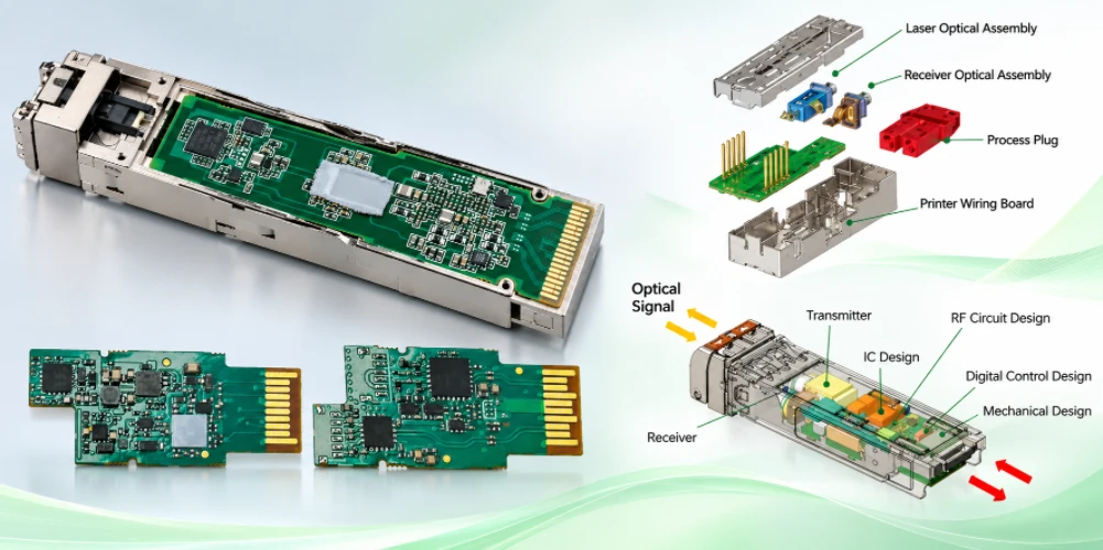
Optical transceiver PCBA and exploded module assembly diagram
SMT, Fine-Pitch Packages and Assembly Process Engineering
Optical transceiver PCBA production may involve fine-pitch BGAs or QFNs, compact passives, precision clocks, dense power-management stages and tightly constrained board outlines. Highleap uses the released component list, PCB land pattern and agreed workmanship criteria to plan printing, placement, reflow and inspection. A generic SMT capability statement does not establish that a particular combination of board thickness, package pitch, finish and testing requirements is ready for production.
The board and assembly must be reviewed as one manufacturing interface. Solder-mask openings, pad metallization, via-in-pad treatment, panel rigidity and handling clearances can determine whether the paste print and solder joints form consistently. Bare-board electrical testing proves neither solder-joint quality nor assembled-board functional performance, so the PCBA plan includes separate process controls and acceptance evidence.
Critical Optical Transceiver SMT Process Controls
- Stencil design and paste deposition: Aperture dimensions and stencil thickness are reviewed for the actual mix of tiny passives, fine-pitch ICs and large thermal pads. Paste release, bridging and insufficient deposits are different risks and should be assessed with the relevant land pattern. If solder-paste inspection is specified, its measurement and disposition criteria are agreed for the build rather than assumed as a universal guarantee.
- Placement data and package verification: Centroid coordinates, rotation, polarity, orientation markings and component height limits must match the actual package variant and assembly revision. A similarly named component with a different footprint or terminal arrangement should not enter production through an informal BOM substitution. First-article placement checks target components whose orientation or clearance errors could make the entire module unusable.
- Reflow and thermal compatibility: The profile must suit the solder alloy, component limits, laminate construction and overall thermal mass. Thin boards, dense copper regions and large exposed pads can heat differently. The production route is reviewed for support fixtures, panel constraints and any secondary operations so components do not experience unauthorized thermal processing simply to accommodate scheduling.
- BGA/QFN solder joints and X-ray evidence: Hidden joints cannot be evaluated solely by visible AOI. X-ray inspection may be appropriate for selected BGA or QFN defects when agreed in the inspection plan, while AOI remains useful for visible placement and solder features. Neither method proves all joint attributes; special tests or destructive evaluation must be separately specified where reliability requirements demand them.
- Via-in-pad and pad-finish coordination: Open vias inside solderable pads may draw solder away from the intended joint. When the approved design needs resin-filled, planarized, copper-capped via-in-pad, that process must be completed at bare-board fabrication and inspected before assembly. Solder-mask plugging is not inherently equivalent. The fabrication and SMT teams coordinate these features before ordering components or cutting stencils.
- Defect handling, rework and process feedback: Tombstoning, solder bridges, voiding, lifted pads or incomplete joints require cause analysis that considers paste geometry, placement, profile, substrate condition and component history. Rework limits and acceptance criteria should be defined for high-value fine-pitch packages; a reworked PCBA is not automatically equivalent to an untouched first article. Significant recurring defects trigger a documented engineering review before volume release.
Release PCBA Quality From Measurable Evidence
When bare-board fabrication and assembly are ordered together, Highleap can coordinate optical transceiver PCB fabrication requirements with pad and via treatment before production. The assembly release then follows the agreed BOM, stencil/placement data, inspection records and board-level test instructions. Complete optical-transceiver module validation remains outside ordinary PCB assembly unless separately specified and confirmed.
OPTICAL TRANSCEIVER PCBA
Ready to Quote Your Transceiver PCBA?
Submit the BOM, released PCB data, centroid files, test scope and planned build quantities for review.
Pricing, process and schedule are confirmed after engineering review.
AOI, X-Ray, Board-Level Testing and Defined Acceptance
Highleap can build the PCBA inspection and testing scope around the customer’s released acceptance requirements. A standard production flow may include incoming checks, solder-paste inspection where applicable, post-placement AOI, X-ray for selected hidden solder joints, and other project-specific checks. The inspection method and lot coverage are agreed according to the package mix and required workmanship standard.
Board-level electrical and functional testing are separate from visual inspection. If the customer requires programming, voltage/current verification, management-interface testing, continuity checks, boundary-scan or a custom functional test, the expected method, firmware, equipment and pass/fail limits should be defined in the RFQ. Highleap can review the provided test procedure and confirm the available process, fixture and responsibility scope before committing to delivery criteria.
A completed optical-transceiver PCBA is not automatically a fully qualified optical transceiver module. Board-level testing does not establish optical coupling alignment, transmitter extinction ratio, receiver sensitivity or BER performance unless those specific tests have been separately engineered, equipped and accepted. These distinctions protect the buyer as well as the manufacturer: the purchase order can state clearly what evidence will accompany the populated board and what will be verified later during module integration.
Documentation can include identified board revision, selected inspection results, first-article records, material/lot traceability or customer-specific reports when required. If the acceptance class, inspection standard or test record format matters to the end product, it should be agreed before production, not added as a surprise requirement before shipment. See Highleap’s X-ray inspection capabilities for the inspection method used in applicable PCBA projects.
Select Inspection Methods to Match Each Failure Mode
SPI can help evaluate paste deposition before placement; AOI is used for visible soldering and placement conditions; X-ray is appropriate for selected hidden joints; electrical or functional testing evaluates the configured board against an approved test sequence. The combination depends on package geometry, assembly method and order acceptance requirements. A claim of “fully tested” is not meaningful unless the test coverage and pass/fail limits are defined. For a transceiver PCBA, a functional test of power rails and digital interfaces is not equivalent to optical power or BER qualification of a completed module.
Fixtures, Programming and Test Data Ownership
If the OEM wants Highleap to run board-level functional tests, the RFQ should include the test procedure, fixture/interface requirements, programming files, expected measurements and acceptance thresholds. The order also identifies who supplies fixtures and software, and whether test records must be returned per serial number or batch. In the absence of this information, the production scope can include assembly inspection without claiming functional coverage that has not been implemented. A prototype fixture may not be suitable for volume throughput; that change is planned with the NPI transition.
NPI Builds, Engineering Changes and Repeat PCBA Production
For a new optical-transceiver PCBA, Highleap’s NPI work aligns the released PCB revision, BOM, placement data, stencil requirements and initial inspection or functional test plan. First builds can reveal missing polarity marks, unsuitable land-pattern assumptions, package handling conflicts or unclear assembly drawings. These findings need documented engineering resolution before the program moves to recurring production.
Changes made during prototype evaluation must remain traceable. If a customer modifies a component footprint, replaces an IC, changes the PCB finish or reroutes a via under a BGA pad, we evaluate the effect on stencil, process settings, component procurement, test coverage and board revision. An approved ECN should travel with the released build package; relying on informal email instructions creates avoidable risk when the production volume increases.
For repeat orders, supply planning addresses component replenishment, approved alternatives, lot separation, customer-owned stock, build scheduling and packing requirements. The delivery commitment must reflect both PCB and component lead times where Highleap supplies the boards. A completed bare-board lot does not necessarily mean the PCBA can be shipped immediately if a long-lead IC is missing or a firmware/test fixture has not been approved.
Highleap can coordinate the assembly work with optical transceiver PCB manufacturing when both scopes are ordered. This creates a clearer route for correcting PCB pad-finish, via-fill or panel issues before they become assembly defects. Our PCBA production acceptance remains tied to the customer’s released assembly and testing requirements, not to a generic claim of full module qualification.
First-Article Builds as Production Validation
The first SMT build confirms more than whether the specified parts were soldered in place. Highleap reviews material readiness, stencil performance, placement orientation, reflow behavior, hidden-joint inspection as required and the customer’s board-level test results. If a repeated defect appears, the response may involve stencil adjustment, PCB land pattern discussion, panel support or a component-handling change, each subject to appropriate design and process approvals. The documented first-article outcome becomes a practical reference for later lots.
ECN Control, Revisions and Line Changeovers
Module programs frequently revise a DSP, connector or power device during development. A BOM revision, PCB artwork revision and assembly program revision must all refer to the same released build. Highleap identifies obsolete part numbers, approved equivalents and any change in assembly sequence before the new lot starts. A seemingly minor connector substitution can alter footprint and soldering requirements; it is not simply a purchasing change. For scheduled repeat orders, component date/lot traceability, protective packing and record retention can be specified in the purchase agreement.
Yield Feedback Into the Bare-Board Specification
If soldering defects recur near fine-pitch devices, the response should not automatically be more aggressive rework. The underlying cause may involve pad geometry, via-in-pad planarity, solder-mask definition, stencil aperture or thermal support. When Highleap supplies both PCB fabrication and assembly, feedback can be traced to the appropriate process owner. Where the OEM supplies bare boards, the same observations can be documented for the customer’s PCB source. This avoids treating production yield as an SMT-only problem when the design or bare-board construction is the actual contributor.
Request an Optical Transceiver PCB Assembly Quote from Highleap
A useful PCBA RFQ includes the released BOM with manufacturer part numbers and approved alternatives, Gerber/ODB++ files, PCB fabrication drawing, centroid/pick-and-place data, assembly drawings, build quantity and requested delivery date. State whether the PCBs and components are to be purchased by Highleap, supplied by the customer or split between the two parties. Identify special components, moisture-sensitive packages, fiducial or panel preferences, conformal coating requirements and critical cosmetic or mechanical constraints.
Production-Ready RFQ Sequence
- Submit the controlled BOM, approved substitutions, component supply ownership and placement data.
- Provide PCB fabrication/finish requirements, panel details and assembly drawings.
- Define firmware, programming, inspection, test-fixture ownership and board-level test limits.
- Confirm pilot quantity, volume forecast and change-control method before production release.
For inspection and testing, provide the intended standard and acceptance class, required X-ray or AOI coverage, firmware/programming files, board-level electrical or functional test procedures, pass/fail limits and any required reporting. If the quote includes module integration or higher-level optical testing, describe those operations explicitly so Highleap can review whether they can be provided as a separately qualified project scope.
Highleap Electronics will review manufacturing data, BOM sourcing, process feasibility, inspection obligations and quantity breaks before confirming the final quotation and production lead time. Submit your optical transceiver PCBA files for a quote with the desired build and delivery scope. We supply customer-defined assembled boards with agreed workmanship and test requirements, supporting the transition from first-article build to reliable repeat production.
RFQ Package for Consigned and Turnkey Assembly
For a meaningful PCBA price, Highleap needs the released PCB data or confirmed board supply route, revision-controlled BOM, approved manufacturers and alternates, centroid file, assembly drawing, target quantity, required delivery date and any special soldering or post-assembly process. Identify parts that will be consigned by the customer and parts that Highleap will purchase. For constrained components, include approved supplier rules and any traceability requirement. If the product needs programming or board-level functional test, supply the procedure, fixtures and pass/fail criteria or ask for a feasibility review.
The quote can then distinguish PCB fabrication, materials, SMT/THT assembly, tooling, inspection and defined testing. If the requested deliverable extends beyond PCBA into optical engine integration or full transceiver qualification, state that explicitly for separate scope confirmation. A transparent scope makes prototype, NPI and repeat-volume offers comparable and reduces unexpected commercial changes after materials have been procured.
OPTICAL TRANSCEIVER PCBA
Ready to Quote Your Transceiver PCBA?
Submit the BOM, released PCB data, centroid files, test scope and planned build quantities for review.
Pricing, process and schedule are confirmed after engineering review.

Recommended Posts
Precision Press Fit PCB Manufacturing with Tight Tolerances
Press-fit PCB manufacturing requires close coordination...
8 Layer HDI PCB Manufacturer in China
Highleap Electronics provides 8 layer HDI PCB...
8 Layer Rigid-Flex PCB Manufacturing and Cost Guide
An 8 layer rigid-flex PCB combines multilayer rigid...
8 Layer PCB Cost in China: Rigid, Flexible & Rigid-Flex Pricing
How much does an 8 layer PCB cost? The answer depends on...
How to get a quote for PCBs
Let‘s run DFM/DFA analysis for you and get back to you with a report. You can upload your files securely through our website. We require the following information in order to give you a quote:
-
- Gerber, ODB++, or .pcb, spec.
- BOM list if you require assembly
- Quantity
- Turn time
In addition to PCB manufacturing, we offer a comprehensive range of electronic services, including PCB design, PCBA, and turnkey solutions. Whether you need help with prototyping, design verification, component sourcing, or mass production, we provide end-to-end support to ensure your project’s success.
For PCBA services, please provide your BOM (Bill of Materials) and any specific assembly instructions. We also offer DFM/DFA analysis to optimize your designs for manufacturability and assembly, ensuring a smooth production process.