
8 Layer Rigid-Flex PCB Manufacturing and Cost Guide
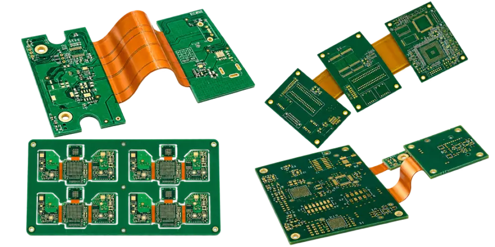
For hardware engineers and PCB buyers, specifying an eight-layer rigid-flex circuit involves more than choosing eight copper layers. The layer distribution between rigid and flexible regions, dielectric construction, copper type, bend geometry, via placement, coverlay openings and stiffeners all influence manufacturability. These decisions also affect quotation accuracy, production lead time and long-term mechanical reliability.
Highleap Electronics supports PCB fabrication and assembly projects that require engineering review, multilayer construction planning and production coordination. This guide focuses on the decisions that matter when sourcing an 8 layer rigid-flex PCB: defining the stackup, controlling the flex zones, reviewing manufacturing requirements, evaluating cost drivers and preparing a complete request for quotation.
Table of Contents
Have an 8 Layer Rigid-Flex PCB Project?
Submit your stackup, fabrication data, bend requirements and order quantity for quotation review.
What Defines an 8 Layer Rigid-Flex PCB?
An eight-layer rigid-flex PCB integrates rigid and flexible circuit regions into one interconnected construction. The rigid sections provide mechanical support for components and dense routing, while the flexible sections connect those regions within the available product envelope. The resulting structure can simplify interconnections, but it must be designed around the electrical and mechanical requirements of the application.
The term 8 layer rigid-flex PCB does not necessarily mean that all eight copper layers continue through every part of the board. A design may have eight copper layers in its rigid sections while using fewer layers in the flexible regions. Other designs may require a more complex regional layer arrangement. The actual construction must be defined by the stackup and fabrication drawing.
This distinction matters when obtaining quotations. If the RFQ specifies only an eight-layer board without showing the layer distribution by zone, different manufacturers may interpret the construction differently. Their prices, proposed materials and manufacturing assumptions may therefore be incomparable.
When Is an Eight-Layer Rigid-Flex Construction Appropriate?
An eight-layer rigid-flex design is worth evaluating when a product requires dense routing across multiple rigid sections but has limited space for conventional cables or board-to-board connectors. Typical applications include:
- Medical electronics: Compact instruments and monitoring equipment that connect multiple circuit sections within a restricted enclosure.
- Aerospace and defense electronics: Assemblies where packaging constraints, interconnection integrity and specified environmental requirements influence the circuit construction.
- Industrial controls: Compact control modules that need interconnected component areas without separate cable assemblies.
- Portable and wearable electronics: Devices where folded geometry, compact packaging and reduced interconnection hardware are important.
- High-density electronic modules: Assemblies requiring multilayer routing in rigid areas and flexible connections between functional sections.
Rigid-flex is not automatically the least expensive solution. If a conventional rigid PCB and cable assembly meet the packaging and reliability requirements, that alternative may be more economical. The decision should compare the complete interconnection system, including board fabrication, connectors, cables, assembly labor and mechanical constraints.
Where rigid sections are not required, an 8 layer flex PCB may be another construction to evaluate.
The construction should therefore be selected according to the actual application rather than the layer count alone. Highleap’s rigid-flex PCB manufacturing and product requirements provide the relevant service context for evaluating a rigid-flex project.
8 Layer Rigid-Flex PCB Stackup and Layer Distribution
The stackup defines how copper layers are arranged, which dielectric materials separate them and how the rigid and flexible regions are integrated. It affects controlled impedance, total thickness, copper balance, mechanical flexibility and the manufacturing sequence.
Before requesting a quotation, engineers should distinguish the overall copper-layer count from the layer configuration in each physical zone. The rigid sections may contain the full multilayer stack, while the flexible regions may use only the layers required for their electrical function. The approved design must show how signals and reference planes connect between these regions.
What the Stackup Drawing Needs to Define
- Rigid-section layer count: Identify the copper layers used for component connections, signal routing, power distribution and reference planes.
- Flexible-section layer count: Specify which signal and reference layers continue through each flex region.
- Dielectric construction: Define the core, prepreg and flexible dielectric arrangement as applicable to the proposed build.
- Finished thickness: Specify the required thickness of the rigid sections and flexible regions separately where they differ.
- Via structure: Identify through vias, blind or buried vias and microvias, including their intended layer connections.
- Impedance requirements: Identify controlled-impedance nets, target values and tolerances, including critical transitions between rigid and flexible regions.
- Regional boundaries: Show where the rigid construction ends, where the flex construction begins and how layers terminate at transitions.
Core thickness, prepreg selection, dielectric spacing and copper distribution must work together to meet electrical requirements. A proposed stackup should be checked for manufacturability and signal integrity before it is released for production.
For multilayer designs, layer thickness and dielectric selection also influence routing geometry and impedance. These variables should be resolved during eight-layer PCB stackup engineering rather than left as assumptions during quotation.
Via Structures and Interlayer Connections
Via selection affects both the electrical routing and the manufacturing route. Through vias connect layers across the board thickness, while blind and buried vias connect selected layers without passing through the entire board. Laser-drilled microvias may be considered where routing density and the selected build-up structure justify them.
Not every eight-layer rigid-flex design needs HDI processing. A conventional through-via structure may be sufficient for some layouts, while dense interconnections may require additional drilling, plating, registration and lamination steps. The RFQ should identify the required via types and layer connections rather than simply stating that the board has eight layers.
When blind or buried vias are part of the design, the manufacturer needs to evaluate the via structure together with the stackup and lamination sequence. The manufacturing and pricing considerations for an eight-layer PCB with blind and buried vias illustrate why via complexity must be specified separately from copper-layer count.
8-LAYER PCB COST & QUOTATION
Get an Accurate Quote for Your 8 Layer PCB
Rigid, flexible, or rigid-flex—your final cost
depends on materials, design complexity,
special processes, and order quantity.
Send Highleap your fabrication files for
a project-specific quotation.
Submit Your PCB Files for a Quote →
Pricing and lead time are confirmed
after engineering review.
Material Selection for Rigid and Flexible Regions
Rigid-flex constructions commonly combine rigid PCB laminate systems with flexible dielectric materials such as polyimide. Depending on the design, the stackup may also include adhesive systems, adhesiveless flexible copper-clad laminates, coverlay and local stiffeners.
The materials must be selected as a coordinated system. Choosing a rigid laminate based only on its price or a flexible material based only on its nominal thickness may overlook bonding compatibility, dielectric performance, bend behavior or the limitations of the intended manufacturing process.
Rigid Laminate Requirements
The rigid sections support components, connectors and dense circuit routing. Material selection should reflect the product’s electrical performance, thermal requirements, finished thickness and reliability targets. The copper distribution and dielectric properties must also support any specified impedance requirements.
For electrically demanding designs, the stackup review should account for trace geometry, reference-plane continuity and the dielectric properties of the selected materials. If a proposed material substitution changes electrical or mechanical performance, it should be approved by the design owner before production.
Flexible Substrate, Coverlay and Adhesive Systems
- Flexible substrate: Evaluate dielectric thickness, copper type and compatibility with the intended static or dynamic bending requirements.
- Copper construction: Select a copper system suitable for the required routing and flex behavior. The choice should be reviewed against the actual bend conditions.
- Coverlay: Define insulation coverage and the openings needed for exposed pads, contacts or other conductive features.
- Bonding materials: Confirm compatibility among the rigid and flexible materials and the specified lamination sequence.
- Stiffeners: Specify local reinforcement where component mounting, connector insertion or assembly handling requires additional support.
Stiffeners should be treated as functional mechanical features, not just additions to the bill of materials. Their thickness, outline and position can influence local rigidity, component support and the usable flex area. A clear stiffener drawing helps the manufacturer understand where reinforcement is required and where bending must remain possible.
For designs that need reinforcement around connectors or component-mounting areas, PCB stiffener construction and placement should be evaluated together with the flex-zone geometry and finished-thickness requirements.
Bend-Zone Design and Mechanical Reliability
The flexible region is often one of the most critical parts of a rigid-flex design. Copper layers, dielectric thickness, bend radius, transition geometry and local reinforcement all influence mechanical strain. A circuit that can be fabricated is not necessarily suitable for repeated dynamic bending.
Before manufacturing, identify whether each flex region is intended for a one-time installation bend, occasional movement or continuous dynamic flexing. These applications impose different design and qualification requirements.
Static Bending Versus Dynamic Flexing
Static flex: The circuit is bent during assembly or installation and is expected to remain in position during normal operation. The design still needs an appropriate bend radius and controlled material transitions, but it does not necessarily require the same fatigue performance as a continuously moving flex circuit.
Dynamic flex: The flexible region repeatedly bends during product operation. Copper construction, dielectric thickness, layer arrangement, bend radius and the location of vias or other stress-concentrating features become especially important. Repeated-flex performance should be evaluated against the expected movement and cycle-life requirements.
For a multilayer flexible region, adding copper layers can increase thickness and mechanical stiffness. An eight-layer rigid-flex PCB should therefore not be assumed to support tight or repeated bending simply because the substrate contains flexible material.
Layout Decisions That Reduce Mechanical Risk
- Control bend radius: Define the minimum radius based on the actual stackup, copper construction and intended flex behavior.
- Review copper distribution: Avoid unnecessary copper features that increase local stiffness or create abrupt changes in mechanical behavior.
- Manage vias and transitions: Avoid placing critical vias or abrupt structural transitions in active bend regions unless the design and manufacturing process explicitly support them.
- Define coverlay openings: Ensure that exposed pads and insulation boundaries match the fabrication data and mechanical requirements.
- Position stiffeners carefully: Reinforce component or connector areas without extending the stiffener into regions intended to bend.
- Specify flex-cycle expectations: For dynamic applications, provide the expected movement, bend geometry and required cycle-life criteria for engineering review.
These are design considerations rather than universal dimensional rules. The acceptable bend radius and feature placement depend on the actual stackup and application. They should be confirmed with the fabricator rather than selected from a generic rule of thumb.
Rigid-to-Flex Transition Design
The transition between a rigid section and a flexible section needs particular attention because the material structure, thickness and mechanical behavior change at this point. The transition should be defined clearly in the fabrication data, including rigid-section boundaries, coverlay configuration, layer termination and stiffener edges where applicable.
Unclear transition geometry can lead to different interpretations during engineering review. It may also affect panelization, registration and inspection planning. Identifying transition regions early helps the manufacturer assess the proposed construction before production is scheduled.
Where the flex section requires laser-drilled features or a tightly controlled via arrangement, drilling strategy and material behavior should be reviewed together. The process requirements for laser drilling in flexible PCB manufacturing are relevant when the proposed design uses laser-formed interconnections or requires special drilling controls.

8 Layer Rigid-Flex PCB Manufacturing Process and Quality Control
Rigid-flex fabrication combines multilayer PCB manufacturing with flexible-circuit processing. The exact route depends on the stackup, material system, regional layer configuration, via structure and required tolerances. Not every eight-layer rigid-flex board uses the same sequence, so the manufacturing plan should be established from the approved design rather than assumed from the layer count.
Engineering Review and CAM Preparation
Before production, the manufacturer reviews the Gerber or ODB++ data, drill files, stackup, fabrication drawing and mechanical information. The review should identify the rigid and flexible regions, layer transitions, coverlay openings, stiffeners, minimum features and special-process requirements.
Any inconsistency between the design files and fabrication notes should be resolved before manufacturing data is released. This is also the stage to confirm material availability, controlled-impedance requirements, inspection scope and whether the requested construction falls within the factory’s qualified capabilities.
Layer Imaging, Drilling and Interconnection
Depending on the approved construction, fabrication may involve inner-layer imaging and etching, multilayer lamination, mechanical drilling, laser drilling, hole-wall preparation, plating and outer-layer pattern formation. Designs that use blind or buried vias or microvias may require additional operations and registration controls.
Via structure should be evaluated alongside the stackup. A conventional through-via construction and a design with multiple blind or buried via levels can require different process routes, even when both are described as eight-layer rigid-flex PCBs.
Lamination, Coverlay and Stiffener Integration
The rigid and flexible materials must be integrated according to the approved construction. Lamination conditions, material compatibility, registration and regional thickness requirements affect the resulting board structure.
Flexible regions may require coverlay application and defined openings, while component or connector areas may need stiffeners. Their placement and dimensions should be specified clearly because they affect both the mechanical structure and subsequent assembly handling.
Surface Finish, Profiling and Electrical Testing
The selected surface finish should match the component interfaces and assembly requirements. Depending on the design, the manufacturing route may also include routing, specialized edge processing, electrical testing and dimensional inspection.
Testing requirements should be agreed before quotation. Electrical continuity and isolation testing are common fabrication requirements, while controlled-impedance verification, microsection analysis, flex reliability tests or special documentation may require additional planning depending on the purchase specification.
Quality Checks for Rigid-Flex Production
- Layer registration: Verify alignment of copper layers and regional features against the applicable tolerances.
- Interconnection integrity: Confirm that specified vias and plated interconnections meet the agreed requirements.
- Thickness and dimensions: Check rigid-section thickness, flex-region thickness and critical mechanical dimensions.
- Coverlay and stiffener placement: Verify openings, bonding areas and reinforcement locations against the fabrication drawing.
- Electrical performance: Perform required continuity, isolation and specified impedance checks.
- Special acceptance criteria: Document any agreed flex-cycle testing, microsection requirements or additional inspection procedures.
Where the application has defined flex reliability or acceptance requirements, those requirements should be documented in the RFQ rather than left for the manufacturer to infer. For flexible and rigid-flex boards, IPC-6013 requirements for flexible and rigid-flex printed boards may be relevant to the agreed qualification and acceptance scope. The applicable revision, class and customer-specific requirements should be confirmed for the actual project.
What Affects 8 Layer Rigid-Flex PCB Cost and Lead Time?
The cost of an eight-layer rigid-flex PCB is determined by its complete manufacturing specification. A comparison based only on finished board size or copper-layer count can be misleading because two boards with similar outlines may have very different material systems, via structures and flexible-region requirements.
- Stackup complexity: Different layer configurations between rigid and flex regions affect material preparation, lamination and registration.
- Material selection: Rigid laminate, flexible copper-clad material, coverlay and bonding systems affect material cost and availability.
- Board dimensions and panel utilization: Outline shape, flex tails, tooling margins and nesting efficiency affect the number of usable boards per production panel.
- Drilling and via structure: Small holes, dense drilling patterns, blind or buried vias and microvias can require additional processing.
- Fine-line requirements: Tight trace/space and registration tolerances may increase process difficulty.
- Surface finish and special processes: Selective hard gold, edge plating, backdrilling, resin filling and other nonstandard requirements can add operations.
- Inspection and documentation: Special electrical tests, reports, traceability and reliability qualification can affect the quotation scope.
- Order quantity: Engineering preparation, tooling and setup costs are spread across different quantities, affecting the unit price.
- Lead-time target: Material availability, engineering approval, lamination sequence and production loading influence the schedule.
For an accurate cost comparison, request quotations at several quantities using the same revision, stackup, surface finish, testing requirements and delivery terms. Do not compare a standard rigid-flex construction with an HDI rigid-flex design that requires additional via processing unless those differences are reflected in the quotation.
Why the Lowest Initial Quote May Not Be the Lowest Project Cost
A preliminary quote may be based on incomplete information. If the fabrication drawing later reveals a special finish, an additional stiffener, a different flex-layer arrangement or a specified reliability test, the supplier may need to revise the quotation and schedule.
Buyers should confirm whether the price is budgetary or engineering-reviewed, which processes are included, and whether tooling, testing, packaging and freight are separate charges. A useful comparison evaluates the quoted scope and the supplier’s ability to meet the agreed specification, not just the headline unit price.
Lead time should also be defined clearly. Ask when the manufacturing clock starts and whether it depends on complete data submission, engineering approval, material confirmation or purchase-order release. These conditions are especially important when a design requires nonstandard materials or a complex rigid-flex construction.
DFM Review and RFQ Requirements for an 8 Layer Rigid-Flex PCB
A complete RFQ package helps manufacturers evaluate the actual construction and reduces the risk of conflicting assumptions between suppliers. Before requesting quotations, prepare the following information.
- Fabrication files: Provide the correct Gerber or ODB++ revision and corresponding NC drill data.
- Stackup drawing: Identify the eight-layer configuration, material types, copper weights, dielectric construction and thickness requirements.
- Rigid and flex zones: Clearly define rigid-section boundaries, flexible regions, layer distribution and transition geometry.
- Bend specifications: State whether the flex is static or dynamic, the required bend radius and any expected cycle-life criteria.
- Mechanical details: Include the board outline, critical dimensions, coverlay openings, stiffener locations and connector requirements.
- Electrical requirements: Specify controlled-impedance nets, target values, tolerances and required electrical verification.
- Via and drilling details: Identify through vias, blind or buried vias, microvias, finished-hole sizes and any filling or capping requirements.
- Surface finish and special processes: Define the required finish, selective plating, edge processing and any nonstandard manufacturing steps.
- Quality requirements: State applicable acceptance criteria, inspection scope, test reports and traceability requirements.
- Commercial requirements: Provide quantities, target delivery date, destination and any approved material alternatives.
Resolve Manufacturing Questions Before Production Release
Before approving the quotation, confirm that the manufacturer has reviewed the stackup, rigid-to-flex transitions, bending conditions, materials and special processes. Ask for clarification where a design feature is close to a process limit or where the fabrication drawing leaves the construction open to interpretation.
A design-for-manufacturing review can identify conflicts involving clearances, drilling, layer registration, coverlay openings and mechanical boundaries before these issues affect production. Highleap’s PCB DFM review is a relevant starting point for discussing manufacturability questions before the order is released.
Any proposed material or geometry change should be approved by the design owner when it could affect electrical performance, mechanical fit or reliability. The quotation should document unresolved questions and distinguish included processes from any additional charges.
Include Assembly Requirements When Buying a Complete PCBA
When the project requires component sourcing and board assembly, provide the BOM, placement data, assembly drawings and test requirements so the full manufacturing scope can be evaluated. A bare-board fabrication quote does not automatically include components, SMT assembly, through-hole assembly or functional testing.
For projects that require both board fabrication and component mounting, PCB assembly services for electronic products can be evaluated alongside the rigid-flex board requirements. The RFQ should make clear whether the requested supply scope is bare boards, assembled PCBs or a broader turnkey arrangement.
Request an 8 Layer Rigid-Flex PCB Manufacturing Quote
Highleap Electronics supports PCB fabrication and assembly projects that require engineering review, multilayer construction planning and manufacturing coordination. For an eight-layer rigid-flex PCB, the quotation should be based on the actual rigid and flexible layer arrangement, selected materials, bending requirements, via structure, surface finish, inspection scope and order quantity.
Submit the fabrication files, stackup drawing, mechanical outline, quantity and target delivery date. Include special impedance, reliability, testing or traceability requirements in the RFQ so they can be reviewed before the quotation is finalized.
Prepare Your Rigid-Flex PCB RFQ
Send your eight-layer stackup, rigid and flex zone details, fabrication data and production requirements for quotation review.
The right eight-layer rigid-flex solution is the one that meets the electrical, mechanical and reliability requirements while remaining practical to manufacture. A clearly defined stackup, documented bend conditions and a complete RFQ package help suppliers evaluate the construction accurately and provide a quotation that reflects the actual project scope.

Recommended Posts

How to Compare 6 Layer PCB Quotes Before Ordering
Comparing 6-layer PCB quotes is not just a matter of...
Quick-Turn 6 Layer PCB Manufacturer in China
Highleap Electronics manufactures six-layer printed...
TG150 PCB Manufacturer for Fabrication and Assembly
Highleap Electronics manufactures TG150 PCB boards to...
TG140 PCB Material Selection and Fabrication
Table of Contents TG140 PCB Materials and Selection...
How to get a quote for PCBs
Let’s run DFM/DFA analysis for you and get back to you with a report. You can upload your files securely through our website. We require the following information in order to give you a quote:
-
- Gerber, ODB++, or .pcb, spec.
- BOM list if you require assembly
- Quantity
- Turn time
For PCBA services, please provide your BOM (Bill of Materials) and any specific assembly instructions. We also offer DFM/DFA analysis to optimize your designs for manufacturability and assembly, ensuring a smooth production process.