
12 Common Rigid-Flex PCB Mistakes That Cause Production Failures

The complexity of rigid-flex PCBs introduces unique design challenges that frequently result in manufacturing failures and reliability issues. These hybrid circuits combine flexible polyimide substrates with traditional rigid FR4 sections, creating specialized requirements that differ significantly from conventional PCB designs.
Understanding these common mistakes enables engineering teams to avoid costly production delays and ensure reliable circuit performance. The following 12 critical rigid-flex PCB mistakes represent the most frequent issues encountered during rigid-flex PCB development and manufacturing.
1. Wrong Prepreg Selection
Standard prepreg materials with high resin content prove unsuitable for rigid-flex applications. Excess resin flows onto flexible sections during lamination, hardening the polyimide and eliminating flexibility. This mistake renders the flex sections inoperable and requires complete board redesign. Use no-flow or low-flow prepreg materials such as 1080 and 106 glass fabrics with at least three prepreg layers to ensure strong interlayer bonding.
2. Inappropriate Flex Core Materials
Selecting adhesive-based flex cores instead of adhesiveless polyimide constructions creates reliability problems under mechanical stress. Adhesive layers represent weak interfaces that promote delamination during flexing operations. Rigid-flex PCB materials require careful selection to ensure mechanical durability and electrical performance. Choose adhesiveless polyimide constructions for superior reliability in dynamic applications.
3. Flex Layers Positioned on Outer Surfaces
Placing flexible layers on board exterior surfaces creates manufacturing difficulties and reliability concerns. Outer flex layers cross low-pressure areas during fabrication, creating uneven surfaces that complicate imaging, etching, and plating processes. This positioning also exposes flex circuits to mechanical damage during handling. Position flex layers at the stackup center with rigid layers providing protection during manufacturing.
4. Asymmetric Layer Construction
Unbalanced copper distribution and dielectric arrangements create mechanical stress during flexing operations. Asymmetric constructions promote warpage and increase delamination risk due to uneven stress distribution across the circuit thickness. Maintain symmetry in both copper weight and dielectric materials throughout the stackup. Pair signal layers with reference planes to control impedance while ensuring balanced mechanical properties.
5. Via Placement in Flex Regions
Positioning vias within flexible areas increases manufacturing costs and reduces reliability. Plated through-holes in flex sections experience mechanical stress during bending, frequently developing barrel cracks that cause intermittent failures. Place all vias in rigid sections at least 20 mils from rigid-flex transition zones. This positioning eliminates mechanical stress on via barrels while simplifying manufacturing processes.
6. Insufficient Bend Radius Calculation
Failing to calculate proper bend radius specifications represents the most critical rigid-flex design error. Insufficient bend radius creates excessive mechanical stress that causes copper fractures and substrate delamination. Follow IPC-2223B standards for bend radius calculations: single-sided flex requires minimum six times total thickness, double-sided flex needs twelve times thickness, and multilayer constructions require twenty-four times thickness.

7. Bend Angles Exceeding 90 Degrees
Designing flex sections with bend angles greater than 90 degrees creates excessive tensile stress on outer radius traces and compression stress on inner radius conductors. These forces increase proportionally with bend angle, accelerating failure mechanisms. Limit bend angles to 90 degrees maximum, particularly for dynamic applications involving repeated flexing. Greater angles require specialized design techniques or alternative mechanical solutions.
8. Sharp Trace Corners in Bend Areas
Routing traces with 45-degree or 90-degree corners in flex sections creates stress concentration points that promote crack initiation. Sharp corners also complicate manufacturing processes and reduce electrical performance at high frequencies. Use curved trace routing throughout flex sections, maintaining smooth transitions without abrupt directional changes. Include dummy traces to provide mechanical reinforcement and improve stress distribution.
9. Abrupt Trace Width Changes
Sudden transitions in trace width, particularly at pad connections, create mechanical weak points that concentrate stress during flexing. These abrupt changes frequently cause conductor failures at connection points. Employ teardrop configurations when connecting traces to pads or vias in flex sections. These tapered transitions distribute mechanical stress while improving electrical connectivity and manufacturing yield.
10. Insufficient Spacing and Clearances
Inadequate spacing between drilled holes and flex transition zones creates stress concentration points that promote tearing and electrical failures. Minimum hole sizes smaller than design specifications increase manufacturing costs and reduce reliability in flex sections. Maintain minimum 50-mil clearance between drilled features and rigid-flex transition zones. Specify minimum 6-mil hole sizes in rigid areas and 7.9-mil minimums in flex sections.
11. Solid Copper Pour in Flex Areas
Using solid copper pours for ground planes in flexible sections eliminates circuit flexibility and creates mechanical stress concentration. Solid copper areas resist bending and frequently crack during flexing operations. Implement cross-hatched ground planes in flex sections to maintain electrical performance while preserving mechanical flexibility. Cross-hatching reduces copper density while providing adequate grounding.
12. Poor Rigid-Flex Interface Management
Inadequate transition zone design creates mechanical discontinuities that concentrate stress and promote failures. Rough material edges and abrupt stiffness changes at interfaces frequently cause conductor damage during flexing. Failing to incorporate stiffeners in areas requiring mechanical support leads to excessive flexing and stress concentration. Extend flex coverlay into rigid regions and include appropriate stiffeners with consistent thickness and positioning.
Preventing Rigid-Flex PCB Mistakes Through Expert Guidance
Successfully avoiding these critical mistakes requires comprehensive understanding of mechanical design principles, material science, and specialized manufacturing processes unique to rigid-flex technology. The complexity of these hybrid circuits demands expertise across multiple engineering disciplines to ensure reliable performance throughout the product lifecycle.
Highleap Electronics provides specialized rigid-flex PCB manufacturing services that address common design and fabrication challenges through experienced engineering support and advanced production capabilities. Our comprehensive approach includes design review, manufacturing optimization, and quality validation procedures that prevent costly mistakes while ensuring superior circuit performance.
Specialized Manufacturing Capabilities:
- Polyimide substrate processing with precise bend radius control and impedance management
- Multi-layer constructions supporting complex geometries with reliable interconnections
- Dynamic flex testing validation with comprehensive cycle life verification
- Advanced inspection techniques including cross-sectional analysis and X-ray evaluation
- Specialized assembly services with appropriate fixturing for complex circuit geometries
Our ISO9001, IATF16949, and ISO14001 certified facilities serve demanding applications in automotive, medical device, aerospace, and telecommunications industries where reliability requirements exceed standard commercial specifications.
Contact our engineering team to discuss your rigid-flex PCB requirements and leverage our expertise to avoid common development mistakes while delivering cost-effective solutions that meet stringent performance expectations.

Recommended Posts
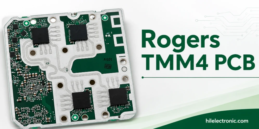
Rogers TMM4 PCB Manufacturer for Compact Microwave Filters
TMM4 is most useful when a microwave circuit must become...

RT/duroid 5870 PCB Manufacturer for Low-Loss PTFE RF Circuits
RT/duroid 5870 is chosen when the RF path needs low loss,...
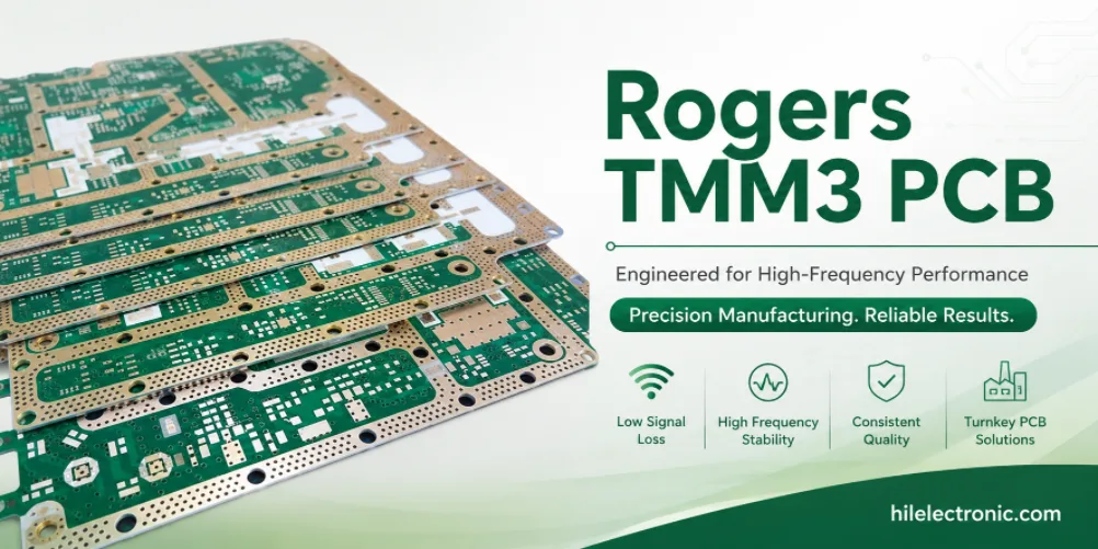
Rogers TMM3 PCB Manufacturer for Mechanical RF Modules
TMM3 is selected when an RF circuit must behave as part of...

Rogers RO3003 PCB Manufacturer for Automotive Radar and mmWave Modules
A 77 GHz radar board is purchased as a working sensor...
How to get a quote for PCBs
Let‘s run DFM/DFA analysis for you and get back to you with a report. You can upload your files securely through our website. We require the following information in order to give you a quote:
-
- Gerber, ODB++, or .pcb, spec.
- BOM list if you require assembly
- Quantity
- Turn time
In addition to PCB manufacturing, we offer a comprehensive range of electronic services, including PCB design, PCBA, and turnkey solutions. Whether you need help with prototyping, design verification, component sourcing, or mass production, we provide end-to-end support to ensure your project’s success.
For PCBA services, please provide your BOM (Bill of Materials) and any specific assembly instructions. We also offer DFM/DFA analysis to optimize your designs for manufacturability and assembly, ensuring a smooth production process.