
8 Layer PCB Cost in China: Rigid, Flexible & Rigid-Flex Pricing
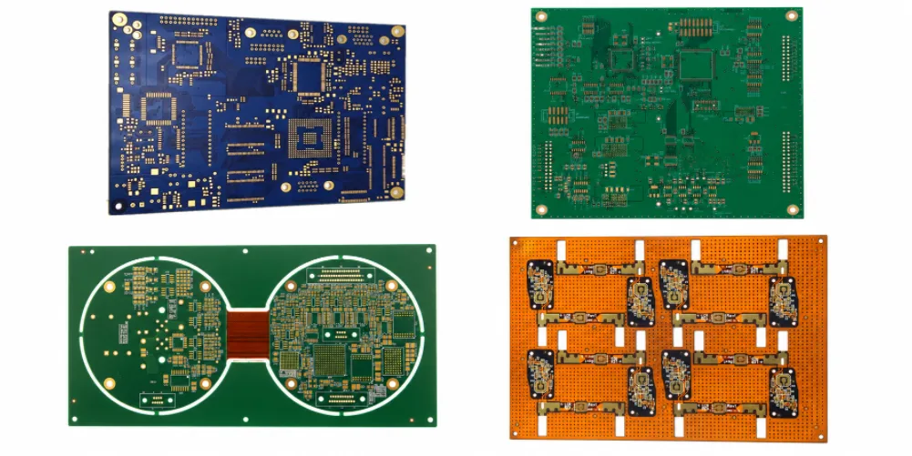
How much does an 8 layer PCB cost? The answer depends on more than the number of copper layers. Board construction, dimensions, laminate grade, copper weight, via structure, surface finish, order quantity and manufacturing requirements all affect the final quotation. A conventional rigid FR-4 eight-layer PCB, an eight-layer flexible circuit and an eight-layer rigid-flex PCB require different materials and production processes, so their prices should not be compared on layer count alone.
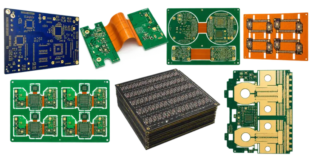
An 8 layer PCB may be a rigid multilayer board, an all-flex circuit or a rigid-flex design that combines rigid sections with flexible interconnections. Even within the same construction category, fine-line routing, small drills, controlled impedance, resin-filled vias, selective plating and special inspection requirements can change the manufacturing route.
For purchasing teams, the objective is to obtain a quotation based on the actual fabrication specification rather than a generic price per layer. This guide explains the main cost drivers for rigid, flexible and rigid-flex eight-layer PCBs, how quantity and lead time affect pricing, which design choices may reduce unnecessary costs, and what information a manufacturer needs to prepare an accurate quote.
Table of Contents
Planning an Eight-Layer PCB Project?
Provide your fabrication files, stackup, quantity and special-process requirements for quotation review.
How Much Does an 8 Layer PCB Cost in 2026?
There is no single reliable price for every eight-layer PCB. A useful estimate requires a defined construction, board size, stackup, material grade, copper weight, minimum trace/space, drilling details, surface finish, order quantity and delivery target. Without these details, a price range may describe a different board from the one a buyer actually needs.
For a conventional rigid FR-4 board, the quotation generally covers multilayer fabrication using the specified laminate, copper distribution, drilling, plating, imaging, etching, solder mask, surface finish, routing and electrical testing. The precise scope depends on the fabrication drawing and the supplier’s quotation terms. Tooling, non-recurring engineering (NRE), special reports, expedited processing, freight, duties and taxes may be charged separately.
For procurement planning, request comparable quotations for the same board revision and specifications at several quantities. A standard rigid PCB quotation should not be used as a direct price reference for a flexible, rigid-flex or HDI construction without accounting for the additional materials and manufacturing steps.
Cost Differences Between Rigid, Flexible and Rigid-Flex PCBs
Rigid 8-layer PCB: The main cost drivers include laminate grade, finished board dimensions, panel utilization, copper weight, drill count and size, surface finish, impedance requirements and inspection scope. A standard FR-4 stackup may suit conventional multilayer electronics, while high-Tg, low-loss or hybrid material systems require separate evaluation.
8-layer flexible PCB: A multilayer flexible circuit uses flexible substrate and conductor materials, typically including polyimide-based construction, with coverlay and other features defined by the design. Total thickness, copper type, coverlay openings, stiffeners and static or dynamic bending requirements can affect both manufacturability and cost. These construction choices are central to calculating flexible PCB fabrication cost.
8-layer rigid-flex PCB: Rigid-flex construction integrates rigid and flexible sections in one circuit. The number of copper layers in each zone, the layers continuing through the bend area, transition geometry, material compatibility and lamination requirements all affect the manufacturing route. There is no universal multiplier that reliably converts a rigid-board price into an eight-layer rigid-flex price. The relevant cost factors are closely tied to the construction and manufacturing cost of a rigid-flex PCB.
Eight-layer HDI boards also require separate evaluation when they use blind or buried vias, laser-drilled microvias, via filling or sequential build-up. These features can change the manufacturing route. For example, pricing an eight-layer PCB with blind and buried vias requires the actual via structure and lamination sequence to be considered rather than the copper-layer count alone.
Practical purchasing rule: Treat preliminary estimates as budgeting references only. A reliable quotation should be based on reviewed manufacturing data, a defined stackup, confirmed quantities and an agreed scope of special processes.
What Factors Affect 8 Layer PCB Manufacturing Cost?
Eight copper layers define the electrical layer count, but they do not fully define the manufacturing process. The quotation depends on the construction type, material consumption, process difficulty, expected yield and inspection requirements. A meaningful comparison starts with the actual stackup and mechanical requirements rather than the layer count alone.
Rigid, Flexible and Rigid-Flex Construction
| Construction Type | Main Cost Drivers | Quotation Details to Confirm |
|---|---|---|
| Rigid 8-layer PCB | Laminate grade, panel utilization, drilling, copper, surface finish and testing. | Finished thickness, material grade, minimum features and via structure. |
| 8-layer flexible PCB | Flexible substrate, copper system, coverlay, registration and stiffeners. | Bending requirements, minimum bend radius, total thickness and stiffener details. |
| 8-layer rigid-flex PCB | Rigid and flex materials, layer distribution, transitions, lamination and bend-zone controls. | Layer count by zone, layers continuing through bends, transition geometry and mechanical requirements. |
An eight-layer rigid-flex PCB commonly has eight layers in its rigid sections, while only selected layers continue through the flexible region. An all-flex circuit with eight copper layers is a different construction. The fabrication drawing and stackup should identify the layer count in each zone clearly; otherwise, suppliers may quote different structures under the same product description.
Rigid-flex can also affect total product cost beyond fabrication. Integrating rigid and flexible sections may eliminate separate connectors, cables or assembly operations in some designs. Where applicable, compare the complete system or assembly cost rather than evaluating the bare board alone. The design must also account for how rigid sections, flexible interconnections, coverlay and stiffeners are coordinated during rigid-flex PCB manufacturing.
Board Size and Panel Utilization
Larger boards generally consume more laminate and production-panel area, but unit cost does not increase in direct proportion to finished board area. The number of boards that fit on a panel, tooling margins, routing allowances, edge clearances and expected panel yield all influence the result.
A long, narrow flex tail or complex board outline may use panel space inefficiently even when the finished circuit has a relatively small area. For a rigid-flex design, the arrangement of rigid sections, flexible tails and coverlay features can also affect panelization and handling.
Materials and Finished Thickness
Standard FR-4 may be an economical option when it meets the product’s electrical, thermal and reliability requirements. High-Tg FR-4, low-loss laminates and mixed-material constructions such as Rogers/FR-4 hybrids may require additional material sourcing, bonding compatibility checks and process qualification.
Flexible and rigid-flex boards add material considerations such as polyimide film, adhesive or adhesiveless copper-clad laminate, coverlay and local stiffeners. Unusual rigid-board thicknesses can limit core and prepreg combinations, while flex thickness affects bending strain and the achievable bend radius.
Core thickness, prepreg selection, copper distribution and dielectric spacing must work together to meet the electrical and mechanical requirements of an eight-layer board. These relationships should be resolved during stackup engineering and design review before the supplier finalizes the manufacturing quotation.
Copper Weight, Drilling and Surface Finish
Higher copper weights, mixed copper thicknesses and demanding trace geometry can require different imaging, etching or plating controls. Hole count, drill size, finished-hole tolerances and plated-hole aspect ratio affect drilling and hole-wall plating. Small drill tools and dense hole patterns can also increase process difficulty.
Surface finishes such as HASL, OSP, ENIG and ENEPIG have different costs and suitability requirements. Selective hard gold for wearing contacts is a separate requirement from ENIG on solderable pads and should be identified explicitly in the fabrication data.
Testing and Documentation Requirements
Controlled-impedance tolerances, dedicated test coupons, microsection reports, traceability and special acceptance criteria may add charges beyond the base fabrication scope. The exact requirements should be agreed before production rather than assumed to be included in a standard board price.
A standard rigid eight-layer board does not automatically require HDI-style sequential lamination; that depends on the interconnection design. Flexible and rigid-flex boards have their own lamination, registration and mechanical reliability requirements. Material consumption, drilling, plating, surface finish and inspection also influence the overall cost of bare PCB fabrication.
How Do Order Quantity and Lead Time Affect 8 Layer PCB Cost?
The 8 layer PCB prototype cost per board is usually higher than the production unit price because engineering review, CAM preparation, tooling setup, purchasing and panel preparation are spread across fewer pieces. Larger orders may improve panel utilization and purchasing efficiency, but the savings depend on a stable design, material availability and actual manufacturing yield.
Flexible outlines and rigid-flex transitions can constrain panel nesting or handling, so a rigid-board volume discount should not automatically be assumed for a flex or rigid-flex design. The manufacturing route and material system must be considered when comparing quantities.
For a useful comparison, request quotations for 10, 100 and 1,000 pieces using the same revision and identical fabrication requirements. These are comparison quantities, not promised price breaks. A different surface finish, via structure, material substitution or inspection scope can make the comparison misleading.
Ask the supplier whether tooling or NRE is charged once, repeated after design changes, or included in the quoted price. Also confirm whether the quoted amount covers bare-board fabrication only or includes any additional inspection, documentation or packaging requirements.
Why Lead Time Affects the Quotation
Lead time depends on the manufacturing route, not just the number of layers. Resin filling, curing, planarization, copper capping, specialized plating and certain lamination processes add steps that cannot always be compressed. Flexible and rigid-flex designs may require additional coverlay lamination, stiffener bonding, rigid-to-flex material processing and bend-related inspection.
Adding one of these requirements after production scheduling can affect both price and delivery. Material availability, engineering clarification, DFM approval, testing scope and the factory’s current production load may also affect the confirmed schedule.
For an urgent order, confirm when the quoted lead time starts: at file submission, receipt of the purchase order, acceptance of complete manufacturing data or final engineering and DFM sign-off. This distinction matters when drawings need clarification or the stackup has not yet been approved. The feasibility of expedited PCB manufacturing should be assessed against the actual construction, material availability and required process sequence.
Total delivered cost = fabrication + tooling/NRE + special-process and specified test charges + expedite fees + freight + applicable duties and taxes.
Compare the total delivered cost rather than the unit price alone. Components and PCB assembly should be quoted separately unless the supplier has explicitly included a combined PCBA scope.
8-LAYER PCB COST & QUOTATION
Get an Accurate Quote for Your 8 Layer PCB
Rigid, flexible, or rigid-flex—your final cost
depends on materials, design complexity,
special processes, and order quantity.
Send Highleap your fabrication files for
a project-specific quotation.
Submit Your PCB Files for a Quote →
Pricing and lead time are confirmed
after engineering review.
How Can PCB Design Choices Reduce 8 Layer PCB Cost?
A design feature can be within a manufacturer’s maximum capability and still be unnecessarily expensive for repeatable production. Using the process limit without a functional reason can reduce throughput, increase scrap risk or require more demanding controls, particularly with specialty laminates or challenging copper constructions.
The objective is not to relax every design rule, but to confirm which tight features are necessary for electrical, mechanical and assembly performance. Reviewing these requirements before fabrication begins can help identify avoidable costs without compromising product reliability.
- Trace and Space: Fine-line imaging and etching can be more demanding, and yield may suffer on some constructions. Use wider geometry where routing density, impedance and current requirements permit. Recalculate controlled impedance before changing trace width or spacing.
- Mechanical Drill Size: Small tools, high hole counts and restrictive aspect ratios can increase process difficulty. Consider whether a 0.30 mm drill tool could replace a 0.20 mm tool where the layout permits. Clarify drill diameter versus finished plated-hole diameter.
- Hole-to-Copper Clearance: Insufficient clearance can threaten nearby copper or create inner-layer shorts. Review annular rings, hole-to-trace spacing and finished-hole tolerances against the fabricator’s DFM rules.
- Vias in Solderable SMT Pads: Solder may wick into open vias and affect assembly yield. Move vias off pads where practical; tenting or plugging is not a universal substitute for a flat, solderable fine-pitch pad.
- Filled-and-Capped Via-in-Pad: Resin filling, curing, planarization and copper capping add process steps. Reserve these processes for designs that require them, and define the required acceptance criteria.
- Layer Distribution Through Flex Zones: More copper layers can increase flex thickness and bending strain. For rigid-flex designs, retain only the necessary signal and reference layers in the bend zone where electrical and mechanical requirements allow.
- Vias and Transitions Near Bend Zones: Stress concentration and transition defects can increase process risk. Keep critical vias and abrupt transitions away from the defined bend region, and review coverlay and stiffener edges.
- Pre-Production DFM Review: Resolve questions about clearances, drilling, material selection and special processes before releasing the order. A PCB design-for-manufacturing review can identify potential manufacturing conflicts before they lead to quotation changes or production delays.
These are cost-conscious design considerations, not universal design-rule limits. A 2/2 mil layout or 0.20 mm drill may be necessary for a particular routing density or electrical requirement. Likewise, a larger drill is not automatically acceptable unless the pad, spacing and interconnect geometry also work.
For fine-pitch BGA layouts, placing vias directly in component pads may improve routing density, but it can also require resin filling, planarization and copper capping. The decision to use via-in-pad construction for fine-pitch PCB layouts should consider assembly requirements, pad geometry and fabrication cost rather than routing density alone.
For flexible circuits, distinguish a one-time installation fold from repeated dynamic flexing. Not every eight-layer flex stackup is suitable for repeated movement, even if it can be manufactured. The required bend radius, flex-cycle expectations, copper construction and mechanical support should be evaluated together.
Which Special PCB Processes Increase Cost or Trigger Re-Quotes?
One avoidable purchasing problem is receiving a low preliminary quote that does not include a special process stated in the fabrication drawing. A supplier may initially estimate a conventional eight-layer board before completing CAM and engineering review. If an omitted requirement is discovered later, the factory may need to revise the price, change the manufacturing route, extend the lead time or decline the job if the specification falls outside its qualified capability.
Before requesting a quotation, check whether the design includes any of the following processes. They should be stated explicitly in the RFQ and confirmed in the supplier’s quotation rather than assumed to be included in a standard eight-layer board price.
- Selective Hard-Gold Plating: Additional masking and plating controls may be required. Gold area, thickness and wear requirements should be defined separately from ENIG.
- Gold Fingers with Beveling: Contact layout, bevel geometry, finish requirements and inspection may require additional processing.
- ENEPIG or Mixed Surface Finishes: Different finishes are not always interchangeable and may require additional processing or masking.
- Resin-Filled and Copper-Capped Vias: Filling, curing, planarization, plating and verification add operations and may affect quick-turn schedules.
- Blind/Buried Vias and Laser Microvias: Additional drilling and registration may be required. Suitable HDI designs may need sequential build-up and lamination.
- Backdrilling: Controlled-depth drilling, dedicated setup and residual-stub measurement requirements can affect cost and delivery.
- Rogers/FR-4 or Other Hybrid Lamination: Material sourcing, bonding compatibility and process qualification may require additional review.
- Heavy or Mixed Copper Weights: Different etching and plating windows may impose restrictions on minimum trace/space.
- Edge Plating, Castellations or Plated Slots: Special routing, plating sequence, panel planning and edge inspection may be necessary.
- Cavities, Stepped Pockets or Counterbores: Controlled-depth machining, special tooling and dimensional verification can add operations.
- Tight-Tolerance Press-Fit Holes: Additional tooling or measurement may be required; feasibility depends on material and finished thickness.
- Flex Coverlay, Stiffeners and Custom Adhesive Patterns: These features can require additional alignment, local bonding, thickness control and inspection.
- Rigid-to-Flex Transitions and Selective Layer Termination: Material processing, lamination planning, registration and bend-zone controls affect the manufacturing route.
- Bend-Cycle Testing or Flex Reliability Qualification: Dedicated test plans, acceptance criteria and qualification requirements can add cost and lead time.
- Special Impedance Reports, Microsections or Traceability: Additional coupons, testing, sampling or documentation may fall outside the base inspection scope.
What Happens if a Special Process Is Missed in the Original Quote?
Consider an eight-layer PCB initially priced with a standard ENIG finish. The fabrication drawing also specifies selective hard-gold plating on an edge connector, including thickness and bevel requirements, but that note is overlooked during the first estimate.
ENIG on solderable pads does not satisfy the selective hard-gold contact requirement. After engineering review, the supplier may need to issue a new quotation and confirm a revised schedule. The same issue can arise when a drawing calls for resin-filled via-in-pad, backdrilling, an unpriced rigid-flex transition, specified flex coverlay and stiffeners, or a hybrid laminate that was not included in the original pricing assumptions.
If a feature set exceeds a factory’s verified process capability, the appropriate response is a technical review, an approved alternative or a clear refusal—not an unsupported manufacturing promise. Buyers should ask whether the quotation is budgetary, subject to DFM review or fully engineering-approved, and request a written list of excluded processes, unresolved capability questions and special-process charges.
Any material substitution, process change, revised price or ship date should be approved before production release. ENIG is commonly used on solderable pads, whereas connector contacts exposed to repeated insertion may require a specified hard-gold finish. Understanding the functional difference between ENIG and hard-gold PCB surface finishes helps prevent incorrect assumptions in the original quotation.
Edge connectors also require the contact geometry, plating specification and any bevel requirements to be defined in the fabrication data. These details are particularly important when applying gold-finger technology to PCB edge connectors, because the contact requirements can introduce additional processing steps.
How Can Buyers Get an Accurate 8 Layer PCB Quote?
A reliable comparison requires the same construction type, board revision, build specification, quantity, quality requirements and delivery terms. An eight-layer rigid PCB quote should not be treated as equivalent to an eight-layer flexible or rigid-flex quote simply because all three contain eight copper layers. A low price based on incomplete assumptions is not the same as an engineering-reviewed quotation for the actual design.
To reduce ambiguity and avoid unnecessary re-quotes, include the following information in the RFQ package:
- Gerber or ODB++ Files and NC Drill Data: Include the correct revision so the supplier can evaluate the copper layers, holes and manufacturing data.
- Fabrication Drawing and Stackup: State material grades, finished thickness, copper weights, dielectric construction and any different rigid and flex zones.
- Construction and Bending Requirements: Identify rigid, all-flex or rigid-flex construction, layer count by zone, static or dynamic bending, minimum bend radius, coverlay and stiffener requirements.
- Minimum Features and Via Requirements: Define trace/space, drill and finished-hole dimensions, blind/buried vias, via-in-pad and required plugging or filling.
- Special Processes and Surface Finishes: List selective hard gold, ENEPIG, resin filling, backdrilling, edge plating, cavities, coverlay openings, special adhesives and other nonstandard steps.
- Quality and Electrical Requirements: Specify applicable acceptance class, controlled impedance, electrical testing, coupons, reports and traceability where needed.
- Quantity and Delivery: Request comparable prototype and production quantities, and state the target delivery date and destination.
- Approved Alternatives: Identify materials or design changes that engineering may consider if they can reduce cost without compromising requirements.
Before placing an order, confirm in writing what the quotation includes, which specifications remain unreviewed, whether all special processes are covered and when the committed lead time begins. If a proposed change affects electrical performance, mechanical fit, assembly or reliability, obtain the design owner’s approval rather than accepting a silent substitution.
If the project also requires assembly, provide the BOM, placement data, assembly drawings and test requirements for a separate or combined PCBA quotation. A bare-board 8 layer PCB price does not automatically include components or SMT assembly. When a project requires both fabrication and component mounting, the required scope can be evaluated through PCB assembly services for electronic products, either separately or alongside the board fabrication requirements.
Request an 8 Layer PCB Cost Estimate from Highleap Electronics
Highleap Electronics reviews rigid, flexible and rigid-flex eight-layer PCB requirements, including layer distribution, material systems, bend conditions, special processes, quantities and delivery targets.
Provide your fabrication files and specifications so manufacturing requirements can be reviewed before the quotation is confirmed.
A dependable PCB quote is not simply the lowest number. It is a price for the correct construction—rigid, flexible or rigid-flex—that has been reviewed against the agreed specification and can be manufactured and delivered on a realistic schedule.

Recommended Posts

5G Small Cell PCB Manufacturing for RF and Telecom Infrastructure
Table of Contents 5G Small Cell PCB Requirements Depend on...
Custom 65% Keyboard PCB and PCBA Manufacturing
Table of contents 1. From Design Files to Production-Ready...
RFSoC Board PCB Manufacturing and Assembly One-Stop Service
Table of contentsReference RFSOC Board Project: 115 × 175...

How to Reduce PCB Costs in 2026
Table of contents Why 80% of PCB Cost Is Locked in at...
How to get a quote for PCBs
Let’s run DFM/DFA analysis for you and get back to you with a report. You can upload your files securely through our website. We require the following information in order to give you a quote:
-
- Gerber, ODB++, or .pcb, spec.
- BOM list if you require assembly
- Quantity
- Turn time
For PCBA services, please provide your BOM (Bill of Materials) and any specific assembly instructions. We also offer DFM/DFA analysis to optimize your designs for manufacturability and assembly, ensuring a smooth production process.