
Ultra Fine Line PCB Manufacturing for High-Density Routing

Ultra fine line PCB manufacturing requires coordinated control of conductor geometry, copper thickness, stack-up and inspection criteria. Highleap Electronics reviews project-specific fabrication data so fine-line requirements can be evaluated in context before quotation.
Send your fabrication data and key requirements for an engineering review. Highleap Electronics can assess the requested construction, clarify manufacturability questions, and prepare a quotation based on the approved scope.
Request an Engineering ReviewPCB Fabrication ServicesUltra Fine Line PCB Manufacturing Starts with Design Rules
“Ultra fine line” is not a universal dimensional class. The actual line/space target, copper thickness, material, layer type and yield expectations must be specified for each project.
State minimum trace width and spacing by layer, and identify whether values apply before or after processing. Review fine-line targets with copper weight and patterning method rather than as an isolated number. If signal loss is also critical, coordinate the design with high-frequency PCB requirements.
“Ultra fine line” is a relative description, not a universal manufacturing specification. The meaningful requirements are the minimum finished conductor width and spacing on each layer, the copper thickness, the intended process route, and the acceptable variation. A target that is achievable on a thin-copper inner layer may not be equivalent to the same nominal line/space on an outer layer with additional copper plating. For that reason, the design rules should be stated by layer and by process condition.
Also distinguish nominal CAD geometry from the finished conductor. The pattern may be affected by resist definition, etching, plating, and local copper density, so the finished line can differ from the drawn line. If the circuit includes fine-pitch escape routing, dense pad fields, or narrow neck-downs, highlight these regions during DFM review. It is better to resolve a small number of critical transitions early than to rely on a generic statement that the whole design is “fine line.”
Copper Thickness, Patterning and Line Geometry
Fine features become harder to control as copper thickness increases relative to line width. Starting copper, plating build-up, resist profile, etching or flash-etch conditions and local pattern density can affect final conductor geometry. The supplier should review the process window before confirming minimum dimensions.
If modified semi-additive processing is required, state it explicitly rather than assuming all suppliers use the same method. Conventional subtractive and mSAP patterning use different process sequences.
1. Why copper thickness changes the achievable line geometry
Fine-line capability is not described by line width and spacing alone. The starting copper foil, copper added during plating, resist thickness and profile, etch compensation, and final surface treatment all influence the conductor shape. As copper thickness increases relative to the target line width, the sidewall profile becomes more difficult to control and the space between adjacent conductors can narrow or vary. Therefore, a line/space value should always be reviewed with the copper weight and layer type attached to it.
Ask whether the stated minimum refers to the design data, the image on the resist, or the finished copper feature. These are not necessarily identical. A quotation based on a nominal CAD dimension may need a process allowance so the finished board meets the electrical and dimensional requirement. State the minimum on each layer separately when outer-layer plating and inner-layer etching use different copper constructions.
2. Subtractive processing, mSAP and SAP are not interchangeable labels
In conventional subtractive processing, a copper-clad base is patterned and unwanted copper is removed. Modified semi-additive processing generally uses a thin conductive seed layer, patterned resist, copper plating in the openings, resist stripping and removal of exposed seed copper. Semi-additive processing also builds conductor features using a seed layer and plating, but its detailed substrate and process sequence may differ. The exact process names and available process windows should be confirmed with the selected fabricator.
For procurement, do not specify mSAP merely because the design is called “fine line.” Provide the target finished geometry and copper requirements, then ask the manufacturer to recommend a qualified process route. If a particular process is mandatory for the design, state it explicitly and confirm that the factory can support the requested material, layer construction, panel size and volume.
3. Line width, spacing and the actual electrical geometry
Trace width affects resistance and current capacity; spacing affects electrical clearance and coupling; and the cross-sectional profile affects both. For controlled impedance, the trace is part of a transmission-line structure that also includes dielectric thickness, dielectric properties, reference-plane geometry and adjacent conductors. A narrow line does not by itself guarantee a target impedance, and reducing spacing can increase crosstalk or create manufacturability risks.
Where high-speed signals are involved, provide target impedance and tolerance, the reference layer, the relevant stack-up, and any differential-pair spacing. The final geometry should be checked against the actual finished copper and dielectric construction. If the laminate or layer thickness changes, the trace dimensions may need to be recalculated rather than copied unchanged from an earlier revision.
4. Layout rules that protect fine-line yield
Review local neck-downs, sharp corners, narrow copper slivers, isolated copper islands, dense pad escapes, solder-mask registration, copper-to-edge clearance and plane clearances. A design may meet a nominal global line/space rule but still contain isolated locations where the geometry is much harder to image or etch consistently. Pay particular attention to transitions around fine-pitch BGA pads, via capture pads and connector footprints.
Panelization and copper distribution matter too. Large areas of copper next to very sparse patterns can create different local process conditions. Include the intended panel constraints if they affect the design and allow the fabricator to recommend compensation where needed. DFM feedback should identify the exact location and dimension in question so the design team can make an informed decision rather than applying a blanket relaxation to the entire board.
5. Inspection and acceptance for fine features
Agree on what will be measured, where it will be measured, and how the result will be reported. AOI can detect many pattern defects, but it does not replace a dimensional acceptance definition for every critical trace. Depending on the project, the plan may include coupons, cross-section review, impedance testing or other electrical verification. Identify which items are required for every lot and which are required only for qualification or first-article approval.
For an ultra-fine-line PCB quotation, provide the data package, stack-up, copper weights, line/space targets by layer, material, finish, impedance table, quantity and expected acceptance records. A useful engineering response should address the proposed process route and identify any design areas that need clarification before release. This makes the quote more reliable than selecting a supplier from a single headline minimum line/space number.
Copper thickness and line geometry must be evaluated together because pattern formation removes or adds copper according to the selected process. In subtractive processing, the starting copper is patterned and etched; the etch profile can influence conductor width and sidewall shape. In additive or modified semi-additive approaches, a thin seed layer and patterned plating sequence can support finer features, but the actual process window depends on the substrate, seed construction, resist, plating, and seed-removal steps. The process name alone does not establish a guaranteed finished line/space.
When requesting a quote, provide both the minimum design line/space and the copper requirements. Identify whether the value is a design target or an acceptance limit on the finished board. Also indicate whether outer layers require additional plated copper and whether the design includes heavy-copper regions adjacent to fine features. Abrupt changes in trace width, dense copper areas, and narrow gaps can make local process control more demanding, so a representative fabrication sample or coupon may be useful where the application justifies it.
Impedance, Crosstalk and Signal Integrity
Smaller traces do not automatically improve signal integrity. Impedance depends on trace geometry, copper thickness, dielectric properties, reference-plane spacing and surrounding stack-up. Fine spacing can also increase coupling and crosstalk if routing and reference planes are not designed appropriately.
Provide target impedance, tolerance, reference layers and relevant frequency or edge-rate context. Use controlled impedance PCB review to consider geometry and stack-up together.
Fine-line routing should be designed in the context of the full transmission-line geometry. Characteristic impedance depends on trace width and thickness, dielectric constant, dielectric height, and the reference-plane configuration. If any of those variables changes during fabrication or stack-up optimization, the resulting impedance can change even when the CAD trace width remains the same. Provide target impedance and tolerance together with the reference layer and the material system.
Spacing is also an electrical design variable. Closely coupled traces may increase crosstalk, and discontinuities around pads, neck-downs, vias, and reference-plane splits can affect signal behavior. For differential pairs, specify pair geometry and the required impedance relationship; for high-speed single-ended nets, identify critical nets and their reference conditions. These requirements should be reviewed with the controlled impedance PCB service as a coordinated stack-up and routing problem, not solved by changing line width alone.

DFM Checks That Protect Fine-Line Yield
A fine-line DFM review should check minimum spacing, neck-downs, acute corners, isolated copper slivers, solder-mask registration, pad-to-trace transitions and layer-specific manufacturability. Copper balancing and panel layout can also affect process stability.
Do not rely on a generic “fine-line capable” claim without a defined stack-up and data set. Share fabrication outputs and use DFM review to identify design-rule conflicts before tooling is released.
A useful DFM review checks more than minimum trace width. It should identify isolated copper slivers, narrow necks, acute corners, insufficient clearances, pad-to-trace transitions, copper features near board edges, solder-mask registration risks, and potential shorts after patterning. The reviewer should also look at the interaction between the fine-line region and the wider copper distribution elsewhere on the same layer. Local density and abrupt transitions can affect process consistency.
Review the finished board requirements as well as the artwork: surface finish, solder-mask openings, test-pad access, and assembly pad geometry may impose constraints on very small features. If the project uses multiple copper weights, verify that the design rules are appropriate for each layer instead of copying one minimum value throughout the stack-up. The DFM review should end with specific questions or changes that can be accepted, rejected, or clarified by the design owner.
Inspection and Acceptance Criteria
Agree how line width and spacing will be verified and what constitutes acceptance. AOI can detect many visible pattern defects, but the inspection plan should match the board construction, feature size and customer requirements.
For critical builds, define coupon requirements, measurement locations, reporting and electrical tests. If the board will be populated, coordinate pad geometry with PCB assembly.
Inspection methods should be chosen according to the feature size and the type of defect that matters. AOI can identify many pattern defects, but the acceptance plan should state the relevant minimum conductor dimensions, spacing, and defect criteria. For critical geometries, the customer and fabricator may need to agree on measurement locations, coupon design, reporting format, and how borderline measurements are treated.
Define the required electrical test separately from visual pattern inspection. Electrical continuity and isolation testing can identify open or short circuits, but it does not necessarily characterize every line-width variation. If impedance is a controlled requirement, specify the coupon or test method and reporting expectation. For assembled boards, make sure the fine-line design also supports solder-mask registration, component land patterns, and the assembly inspection strategy.
Request an Ultra Fine Line PCB Quote
Submit Gerber or ODB++ data, stack-up, copper weights, minimum line/space by layer, material, surface finish, impedance table, board dimensions, quantity and target date. If the design is early-stage, provide target dimensions and electrical requirements so feasibility can be discussed before routing is frozen.
For fabrication and assembly, include BOM and pick-and-place data. Start at the PCB quotation page and review PCB fabrication services.
For a useful quotation, provide Gerber or ODB++ data, a complete stack-up, copper weight by layer, minimum line/space by layer, material, finished thickness, surface finish, impedance requirements, board outline, quantity, and delivery target. Identify the most critical features and explain whether the specified line/space values are nominal design rules or guaranteed finished-board acceptance limits. If there is a customer specification or drawing standard, include its revision.
If the design is still in development, share the intended function, component pitch, critical net requirements, and any flexibility in line/space or material. This helps the engineering review distinguish must-have requirements from preferences that may be adjusted to improve manufacturability or cost. If assembly is included, add the BOM, placement data, assembly drawing, and test requirements so the full project scope can be quoted rather than treating the bare board as the only deliverable.
Frequently Asked Questions
What line and space can you manufacture?
The feasible minimum depends on copper thickness, layer, material, process route, panel layout and acceptance criteria. Submit the stack-up and data for engineering review.
Does ultra fine line always require mSAP?
No. The suitable process depends on requested geometry and construction. The fabricator should review whether subtractive, mSAP or another qualified process is appropriate.
What information is most important for quoting?
Minimum line/space by layer, copper weights, stack-up, material, impedance needs, board size, quantity, finish and delivery target.
Discuss Your Ultra Fine Line PCB Manufacturing Project
Share current Gerber files, stack-up or mechanical drawing, fabrication notes, quantity, target date and acceptance criteria. We will review the supplied information and identify details needed to quote the build responsibly.
Request a PCB QuoteAdd PCB AssemblyEngineering note: manufacturability, achievable dimensions, tolerances, materials, inspection methods and lead time depend on the specific design and production review. Confirm critical requirements in the approved fabrication package before release.

Recommended Posts
24 Layer PCB Manufacturer in China
How to get a quote for PCBs Let‘s run DFM/DFA analysis for...
Stacked Microvia PCB Manufacturing
How to get a quote for PCBs Let‘s run DFM/DFA analysis for...
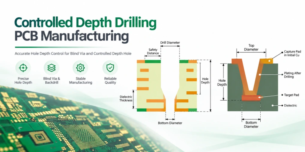
Controlled-Depth Drilling PCB Manufacturing
How to get a quote for PCBs Let‘s run DFM/DFA analysis for...
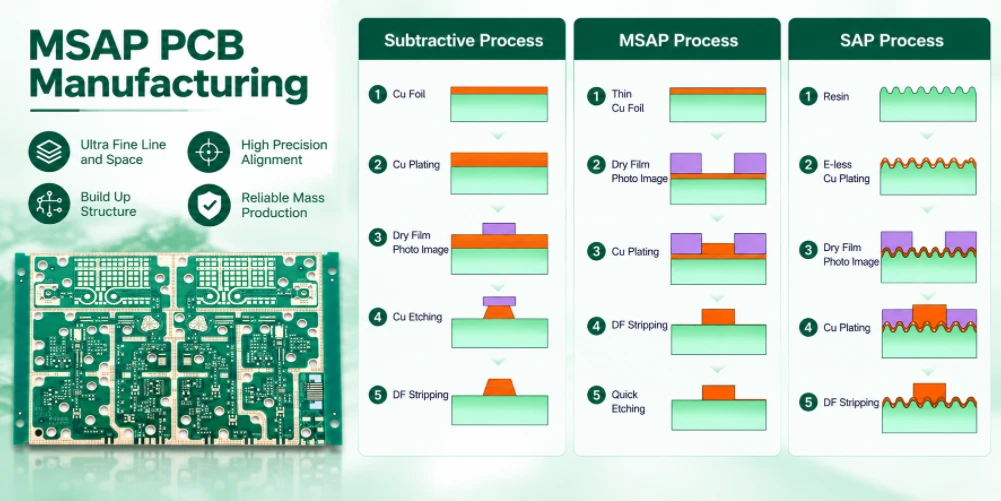
mSAP PCB Manufacturing for Fine-Line Circuitry
Highleap Electronics provides mSAP PCB manufacturing...
How to get a quote for PCBs
Let‘s run DFM/DFA analysis for you and get back to you with a report. You can upload your files securely through our website. We require the following information in order to give you a quote:
-
- Gerber, ODB++, or .pcb, spec.
- BOM list if you require assembly
- Quantity
- Turn time
In addition to PCB manufacturing, we offer a comprehensive range of electronic services, including PCB design, PCBA, and turnkey solutions. Whether you need help with prototyping, design verification, component sourcing, or mass production, we provide end-to-end support to ensure your project’s success.
For PCBA services, please provide your BOM (Bill of Materials) and any specific assembly instructions. We also offer DFM/DFA analysis to optimize your designs for manufacturability and assembly, ensuring a smooth production process.